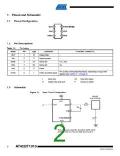
1. Pinout and Schematic
1.1
Pinout Configuration
OUT
VSS
1
2
3
6
5
4
SYNC/MODE
VDD
SNSK
SNS
1.2
Pin Descriptions
Table 1-1.
Name
OUT
Pin Listing
Pin
1
Type
O
Comments
If Unused, Connect To...
Output state
–
Vss
2
P
Supply ground
Sense pin
Sense pin
Power
–
SNSK
SNS
3
I/O
I/O
P
Cs + Key
4
Cs
–
Vdd
5
Pin is either SYNC/Slow/Fast Mode, depending on logic level
applied (see Section 3.1 on page 4)
SYNC
6
I
SYNC and Mode Input
I
Input only
I/O
P
Input and output
Ground or power
O
Output only, push-pull
1.3
Schematic
Figure 1-1. Basic Circuit Configuration
VDD
5
SENSE
ELECTRODE
VDD
Rs
1
3
4
OUT
SNSK
SNS
Cs
6
Cx
SYNC/MODE
VSS
2
Note: A bypass capacitor should be tightly wired
between Vdd and Vss and kept close to pin 5.
2
AT42QT1010
9541G–AT42–03/10

 ATMEL [ ATMEL ]