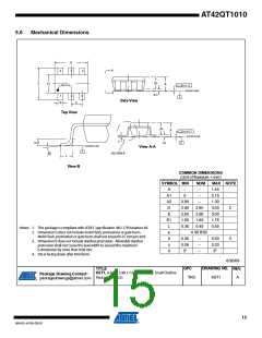
5. Specifications
5.1
Absolute Maximum Specifications
Operating temperature
-40°C to +85°C
-55°C to +125°C
0 to +6.5V
Storage temperature
VDD
Max continuous pin current, any control or drive pin
Short circuit duration to Vss, any pin
Short circuit duration to Vdd, any pin
Voltage forced onto any pin
±20 mA
Infinite
Infinite
-0.6V to (VDD + 0.6) Volts
CAUTION: Stresses beyond those listed under Absolute Maximum Specifications may cause permanent damage to the
device. This is a stress rating only and functional operation of the device at these or other conditions beyond those
indicated in the operational sections of this specification is not implied. Exposure to absolute maximum specification
conditions for extended periods may affect device reliability
5.2
Recommended Operating Conditions
VDD
Short-term supply ripple + noise
+1.8 to 5.5V
±20 mV
Long-term supply stability
Cs value
±100 mV
2 to 50 nF
5 to 50 pF
Cx value
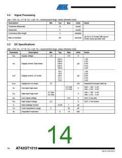
5.3
AC Specifications
Vdd = 3.0V, Cs = 4.± nF, Cx = 5 pF, Ta = recommended range, unless otherwise noted
Parameter
TRC
Description
Recalibration time
Min
Typ
200
3.05
9.0
Max
Units
ms
Notes
Cs, Cx dependent
TPC
Charge duration
Transfer duration
µs
±±.5% spread spectrum variation
±±.5% spread spectrum variation
TPT
µs
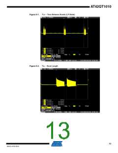
Time between end of burst and
start of the next (Fast mode)
TG1
TG2
TBL
1.2
80
ms
ms
ms
Time between end of burst and
start of the next (LP mode)
Increases with decreasing VDD
See Figure 5-1 on page 13
VDD, Cs and Cx dependent. See
Section 4.2 for capacitor selection.
Burst length
2.45
TR
Response time
100
ms
µs
THB
HeartBeat pulse width
15
12
AT42QT1010
9541G–AT42–03/10

 ATMEL [ ATMEL ]