8.
Write Operations
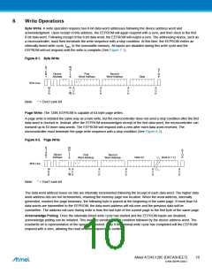
Byte Write: A write operation requires two 8-bit data word addresses following the device address word and
acknowledgment. Upon receipt of this address, the EEPROM will again respond with a zero, and then clock in the first
8-bit data word. Following receipt of the 8-bit data word, the EEPROM will output a zero. The addressing device, such as
a microcontroller, must then terminate the write sequence with a stop condition. At this time, the EEPROM enters an
internally-timed write cycle, tWR, to the nonvolatile memory. All inputs are disabled during this write cycle and the
EEPROM will not respond until the write is complete (See Figure 7-1).
Figure 8-1. Byte Write
S
T
A
R
T
W
R
I
S
T
Device
First
Second
T
E
O
P
Data
Address
Word Address
Word Address
SDA Line
M
S
B
R A
A
C
K
A
C
K
A
C
K
/
C
W K
Note: * = Don’t care bit
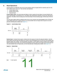
Page Write: The 128K EEPROM is capable of 64-byte page writes.
A page write is initiated the same way as a byte write, but the microcontroller does not send a stop condition after the first
data word is clocked in. Instead, after the EEPROM acknowledges receipt of the first data word, the microcontroller can
transmit up to 63 more data words. The EEPROM will respond with a zero after each data word received. The
microcontroller must terminate the page write sequence with a stop condition (See Figure 8-2).
Figure 8-2. Page Write
S
T
A
R
T
W
R
I
S
T
Device
First
Second
T
E
O
P
Address
Data (n)
Data (n + x)
Word Address
Word Address
SDA Line
M
S
B
R A
/ C
A
C
K
A
C
K
A
C
K
A
C
K
W K
Note: * = Don’t care bit
The data word address lower six bits are internally incremented following the receipt of each data word. The higher data
word address bits are not incremented, retaining the memory page row location. When the word address, internally
generated, reaches the page boundary, the following byte is placed at the beginning of the same page. If more than 64
data words are transmitted to the EEPROM, the data word address will roll-over and the previous data will be
overwritten. The address roll-over during write is from the last byte of the current page to the first byte of the same page.
Acknowledge Polling: Once the internally-timed write cycle has started and the EEPROM inputs are disabled,
acknowledge polling can be initiated. This involves sending a start condition followed by the device address word. The
read/write bit is representative of the operation desired. Only if the internal write cycle has completed will the EEPROM
respond with a zero, allowing the read or write sequence to continue.
Atmel AT24C128C [DATASHEET]
10
8734B–SEEPR–9/2012

 ATMEL [ ATMEL ]