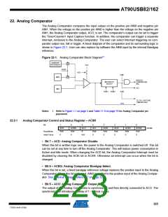
• Bit 4 – ACI: Analog Comparator Interrupt Flag
This bit is set by hardware when a comparator output event triggers the interrupt mode defined
by ACIS1 and ACIS0. The Analog Comparator interrupt routine is executed if the ACIE bit is set
and the I-bit in SREG is set. ACI is cleared by hardware when executing the corresponding inter-
rupt handling vector. Alternatively, ACI is cleared by writing a logic one to the flag.
• Bit 3 – ACIE: Analog Comparator Interrupt Enable
When the ACIE bit is written logic one and the I-bit in the Status Register is set, the Analog Com-
parator interrupt is activated. When written logic zero, the interrupt is disabled.
• Bit 2 – ACIC: Analog Comparator Input Capture Enable
When written logic one, this bit enables the input capture function in Timer/Counter1 to be trig-
gered by the Analog Comparator. The comparator output is in this case directly connected to the
input capture front-end logic, making the comparator utilize the noise canceler and edge select
features of the Timer/Counter1 Input Capture interrupt. When written logic zero, no connection
between the Analog Comparator and the input capture function exists. To make the comparator
trigger the Timer/Counter1 Input Capture interrupt, the ICIE1 bit in the Timer Interrupt Mask
Register (TIMSK1) must be set.
• Bits 1, 0 – ACIS1, ACIS0: Analog Comparator Interrupt Mode Select
These bits determine which comparator events that trigger the Analog Comparator interrupt. The
different settings are shown in Table 22-1.
Table 22-1. ACIS1/ACIS0 Settings
ACIS1
ACIS0
Interrupt Mode
0
0
1
1
0
1
0
1
Comparator Interrupt on Output Toggle.
Reserved
Comparator Interrupt on Falling Output Edge.
Comparator Interrupt on Rising Output Edge.
When changing the ACIS1/ACIS0 bits, the Analog Comparator Interrupt must be disabled by
clearing its Interrupt Enable bit in the ACSR Register. Otherwise an interrupt can occur when the
bits are changed.
22.0.2
Digital Input Disable Register 1 – DIDR1
Bit
7
6
5
–
R
0
4
–
R
0
3
–
R
0
2
–
R
0
1
0
–
–
AIN1D
R/W
0
AIN0D
R/W
0
DIDR1
Read/Write
Initial Value
R
0
R
0
• Bit 1, 0 – AIN1D, AIN0D: AIN1, AIN0 Digital Input Disable
When this bit is written logic one, the digital input buffer on the AIN1/0 pin is disabled. The corre-
sponding PIN Register bit will always read as zero when this bit is set. When an analog signal is
applied to the AIN1/0 pin and the digital input from this pin is not needed, this bit should be writ-
ten logic one to reduce power consumption in the digital input buffer.
224
AT90USB82/162
7707D–AVR–07/08

 ATMEL [ ATMEL ]