AT90USB64/128
24. Analog Comparator
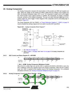
The Analog Comparator compares the input values on the positive pin AIN0 and negative pin
AIN1. When the voltage on the positive pin AIN0 is higher than the voltage on the negative pin
AIN1, the Analog Comparator output, ACO, is set. The comparator’s output can be set to trigger
the Timer/Counter1 Input Capture function. In addition, the comparator can trigger a separate
interrupt, exclusive to the Analog Comparator. The user can select Interrupt triggering on com-
parator output rise, fall or toggle. A block diagram of the comparator and its surrounding logic is
shown in Figure 24-1.
The Power Reduction ADC bit, PRADC, in “Power Reduction Register 0 - PRR0” on page 55
must be disabled by writing a logical zero to be able to use the ADC input MUX.
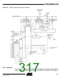
Figure 24-1. Analog Comparator Block Diagram(2)
BANDGAP
REFERENCE
ACBG
ACME
ADEN
ADC MULTIPLEXER
OUTPUT(1)
Notes: 1. See Table 24-2 on page 315.
2. Refer to Figure 1-1 on page 3 and Table 10-6 on page 81 for Analog Comparator pin
placement.
24.0.1
ADC Control and Status Register B – ADCSRB
Bit
7
6
5
4
–
R
0
3
-
2
1
0
–
ACME
–
ADTS2
R/W
0
ADTS1
R/W
0
ADTS0
R/W
0
ADCSRB
Read/Write
Initial Value
R
0
R/W
0
R
0
R
0
• Bit 6 – ACME: Analog Comparator Multiplexer Enable
When this bit is written logic one and the ADC is switched off (ADEN in ADCSRA is zero), the
ADC multiplexer selects the negative input to the Analog Comparator. When this bit is written
logic zero, AIN1 is applied to the negative input of the Analog Comparator. For a detailed
description of this bit, see “Analog Comparator Multiplexed Input” on page 315.
24.0.2
Analog Comparator Control and Status Register – ACSR
Bit
7
6
5
4
3
2
1
0
ACD
ACBG
ACO
ACI
ACIE
R/W
0
ACIC
R/W
0
ACIS1
R/W
0
ACIS0
R/W
0
ACSR
Read/Write
Initial Value
R/W
0
R/W
0
R
R/W
0
N/A
• Bit 7 – ACD: Analog Comparator Disable
313
7593A–AVR–02/06

 ATMEL [ ATMEL ]