AT90USB64/128
nine data bits, then the ninth bit (RXB8n) is used for identifying address and data frames. When
the frame type bit (the first stop or the ninth bit) is one, the frame contains an address. When the
frame type bit is zero the frame is a data frame.
The Multi-processor Communication mode enables several slave MCUs to receive data from a
master MCU. This is done by first decoding an address frame to find out which MCU has been
addressed. If a particular slave MCU has been addressed, it will receive the following data
frames as normal, while the other slave MCUs will ignore the received frames until another
address frame is received.
18.8.1
Using MPCMn
For an MCU to act as a master MCU, it can use a 9-bit character frame format (UCSZn = 7). The
ninth bit (TXB8n) must be set when an address frame (TXB8n = 1) or cleared when a data frame
(TXB = 0) is being transmitted. The slave MCUs must in this case be set to use a 9-bit character
frame format.
The following procedure should be used to exchange data in Multi-processor Communication
mode:
1. All Slave MCUs are in Multi-processor Communication mode (MPCMn in UCSRnA is
set).
2. The Master MCU sends an address frame, and all slaves receive and read this frame.
In the Slave MCUs, the RXCn Flag in UCSRnA will be set as normal.
3. Each Slave MCU reads the UDRn Register and determines if it has been selected. If
so, it clears the MPCMn bit in UCSRnA, otherwise it waits for the next address byte and
keeps the MPCMn setting.
4. The addressed MCU will receive all data frames until a new address frame is received.
The other Slave MCUs, which still have the MPCMn bit set, will ignore the data frames.
5. When the last data frame is received by the addressed MCU, the addressed MCU sets
the MPCMn bit and waits for a new address frame from master. The process then
repeats from 2.
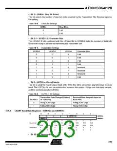
Using any of the 5- to 8-bit character frame formats is possible, but impractical since the
Receiver must change between using n and n+1 character frame formats. This makes full-
duplex operation difficult since the Transmitter and Receiver uses the same character size set-
ting. If 5- to 8-bit character frames are used, the Transmitter must be set to use two stop bit
(USBSn = 1) since the first stop bit is used for indicating the frame type.
Do not use Read-Modify-Write instructions (SBI and CBI) to set or clear the MPCMn bit. The
MPCMn bit shares the same I/O location as the TXCn Flag and this might accidentally be
cleared when using SBI or CBI instructions.
18.9 USART Register Description
18.9.1
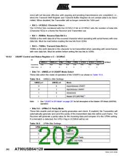
USART I/O Data Register n– UDRn
Bit
7
6
5
4
3
2
1
0
RXB[7:0]
TXB[7:0]
R/W
UDRn (Read)
UDRn (Write)
Read/Write
Initial Value
R/W
0
R/W
0
R/W
0
R/W
0
R/W
0
R/W
0
R/W
0
0
The USART Transmit Data Buffer Register and USART Receive Data Buffer Registers share the
same I/O address referred to as USART Data Register or UDRn. The Transmit Data Buffer Reg-
199
7593A–AVR–02/06

 ATMEL [ ATMEL ]