AT89C4051
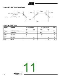
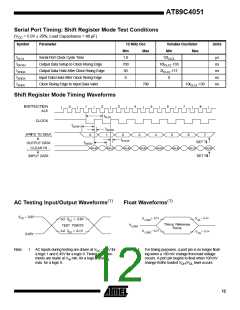
Serial Port Timing: Shift Register Mode Test Conditions
(VCC = 5.0V ± 20%; Load Capacitance = 80 pF)
Symbol
Parameter
12 MHz Osc
Variable Oscillator
Units
Min
Max
Min
12tCLCL
10tCLCL-133
2tCLCL-117
0
Max
tXLXL
tQVXH
tXHQX
tXHDX
tXHDV
Serial Port Clock Cycle Time
1.0
700
50
0
µs
ns
ns
ns
ns
Output Data Setup to Clock Rising Edge
Output Data Hold After Clock Rising Edge
Input Data Hold After Clock Rising Edge
Clock Rising Edge to Input Data Valid
700
10tCLCL-133
Shift Register Mode Timing Waveforms
(1)
(1)
AC Testing Input/Output Waveforms
Float Waveforms
Note:
1. AC Inputs during testing are driven at VCC - 0.5V for
a logic 1 and 0.45V for a logic 0. Timing measure-
ments are made at VIH min. for a logic 1 and VIL
max. for a logic 0.
Note:
1. For timing purposes, a port pin is no longer float-
ing when a 100 mV change from load voltage
occurs. A port pin begins to float when 100 mV
change frothe loaded V /V level occurs.
OH OL
12

 ATMEL [ ATMEL ]