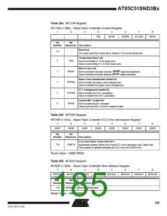
•
or illegal operation (ILGLI)
–
Attempt to access a NF device which is not declared (e.g. DEV= 4 while
NUMDEV= 2)
–
Write of events (NFDATF, NFDAT, NFCMD, NFADC, NFADR) while NFC is
running (NFRUN= 1).
Note that writing in NFACT while NFC is running (RUN=1) does not lead to
an ILGLI interrupt.
As soon as an enabled interrupt is triggered, the NFC becomes not running
(NFRUN= 0).
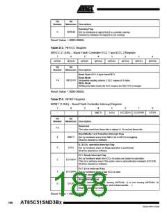
Registers
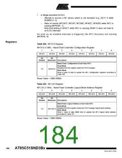
Table 202. NFCFG Register
NFCFG (1.99h) – Nand Flash Controller Configuration Register
7
6
5
4
3
2
1
0
NFGD7
NFGD6
NFGD5
NFGD4
NFGD3
NFGD2
NFGD1
NFGD0
Bit
Bit
Number
Mnemonic Description
Nand Flash Configuration 8-byte Data FIFO
Read Mode
Reading from this register resets the FIFO manager.
7-0
NFGD7:0
Write Mode
Write 8 bytes of data to update the NFC configuration registers according to
Table 188.
Reset Value = 0000 0000b
Table 203. NFLOG Register
NFLOG (1.9Ah) – Nand Flash Controller Logical Block Address Register
7
6
5
4
3
2
1
0
NFLAD7
NFLAD6
NFLAD5
NFLAD4
NFLAD3
NFLAD2
NFLAD1
NFLAD0
Bit
Bit
Number
Mnemonic Description
Nand Flash Logical Address 2-byte Data FIFO
Read Mode
Reading from this register resets the FIFO manager logical block address.
Write Mode
7-0
NFLAD7:0
Write 2 bytes of data (MSB first) to update the NFC logical block address
according to Table 197.
Reset Value = 0000 0000b
184
AT85C51SND3Bx
7632A–MP3–03/06

 ATMEL [ ATMEL ]