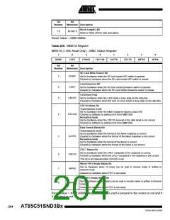
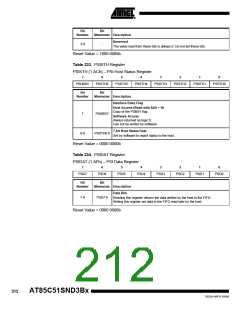
PSI Addressing
The AT85C51SND3Bx are accessible by a host in read or write at two different address
locations by setting or clearing the SA0 address signal. The data management is
detailed in following sections and differs depending on SA0 level. Table 234 shows the
addressing truth table. Figure 100 and Figure 101 show the read and write host cycles.
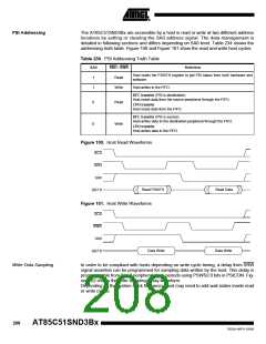
Table 230. PSI Addressing Truth Table
SA0
1
SRD / SWR
Read
Selection
Host reads the PSISTH register to get PSI status from both hardware and
software.
1
Write
Host writes in the FIFO.
DFC transfer (PSI is destination)
Host reads data from the source peripheral through the FIFO.
0
0
Read
Write
CPU transfer
Host reads data from the FIFO.
DFC transfer (PSI is source)
Host writes data to the destination peripheral through the FIFO.
CPU transfer
Host writes data in the FIFO.
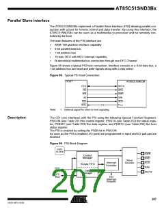
Figure 100. Host Read Waveforms
SCS
SRD
SA0
Read PSISTH
Read Data
SD7:0
Figure 101. Host Write Waveforms
SCS
SWR
SA0
Data Write
Data Write
SD7:0
Write Data Sampling
In order to be compliant with hosts depending on write cycle timing, a delay from SRW
signal assertion can be programmed for sampling data written by the host. This delay is
programmable from 0 to 7 peripheral clock periods using PSWS2:0 bits in PSICON. Fig-
ure 102 shows the write sampling delay waveform.
Depending on the system clock frequency, host may need to add wait states inside read
or write cycles.
208
AT85C51SND3Bx
7632A–MP3–03/06

 ATMEL [ ATMEL ]