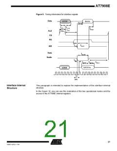
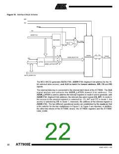
Figure 10. Interface Block Scheme
WR
RD
MODE
CS
ADDR<7:0>
DECODER
1
0
CS_CASA
CS_INT
CASA2
REGISTER
CASA2
CAN_CORE
ADDR_REG<7:0>
ALE
1
0
LATCH
ADDR_LATCH<7:0>
DATA_ADDR<7:0>
The MCU 80C32 generates DATA<7:0>, ADDR<7:0> (highest 8-bit address for the 16-
bit external data access), and ALE to latch the lowest address, WR, CS and RD
signals.
The external data bus is connected to the internal latch block of the AT7908E. The ALE
signal latches and extracts the ADDR_LATCH (lowest 8-bit address). The
ADDR_LATCH is used to address the internal registers in mode 0 and to generate, with
ADDR<7:0> (highest 8-bit address), the internal chip select signal (CS_INT). In mode 0,
the access to the internal registers is selected by CS_INT and CS; in mode 1, the
access is selected by CS. In mode 1, moreover, the address of the internal register is
ADDR<7:0>. The two different operational modes are established by the mode pin that
is the selector for the two multiplexers in Figure 5. In Figure 5 are reported, in addition,
the other two blocks of the AT7908E device: the AT7908E registers and the AT7908E
CAN_CORE.
22
AT7908E
4268D–AERO–11/09

 ATMEL [ ATMEL ]