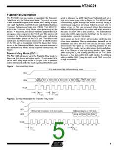
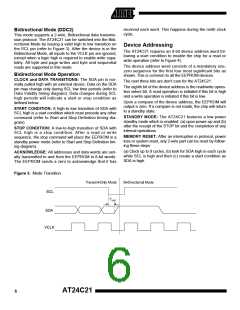
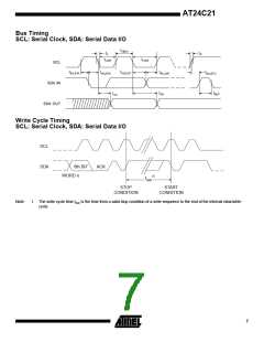
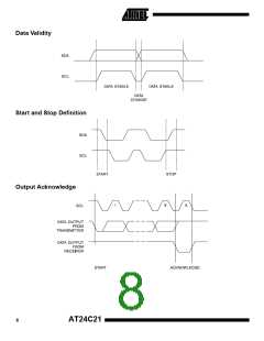
AT24C21
WRITE PROTECTION: When VCLK pin is connected to
GND and in the Bidirectional Mode, the entire memory is
protected and becomes ROM only. This protects the device
memory from any inadvertent write operations.
Write Operations
BYTE WRITE: A write operation requires an 8-bit data
word addresses following the device address word and
acknowledgment. Upon receipt of this address, the
EEPROM will again respond with a zero and then clock in
the first 8-bit data word. Following receipt of the 8-bit data
word, the EEPROM will output a zero and the addressing
device, such as a microcontroller, must terminate the write
sequence with a stop condition. At this time the EEPROM
enters an internally-timed write cycle , tWR, to the nonvola-
tile memory. All inputs are disabled during this write cycle
and the EEPROM will not respond until the write is com-
plete (refer to Figure 5).
NOISE PROTECTION: Special internal circuitry placed on
the SDA and SCL pins prevent small noise spikes from
activating the device. Furthermore, the AT24C21 employs
a low VCC detector circuit which disables the erase\write
logic whenever VCC falls below 1.5 volts.
Read Operations
Read operations are initiated the same way as write opera-
tions with the exception that the read/write select bit in the
device address word is set to one. There are three read
operations: current address read, random address read
and sequential read.
It is required that VCLK be held at a high logic level in order
to program the device. This applies to byte write and page
write operation. Note that VCLK can go low while the
device is in its self-timed program operation and not affect
programming.
CURRENT ADDRESS READ: The internal data word
address counter maintains the last address accessed dur-
ing the last read or write operation, incremented by one.
This address stays valid between operations as long as the
chip power is maintained. The address “roll over” during
read is from the last byte of the last memory page to the
first byte of the first page.
PAGE WRITE: The AT24C21 is capable of an 8-byte page
write.
A page write is initiated the same as a byte write, but the
microcontroller does not send a stop condition after the first
data word is clocked in. Instead, after the EEPROM
acknowledges receipt of the first data word, the microcon-
troller can transmit up to seven more data words. The
EEPROM will respond with a zero after each data word
received. The microcontroller must terminate the page
write sequence with a stop condition (refer to Figure 6).
Once the device address with the read/write select bit set
to one is clocked in and acknowledged by the EEPROM,
the current address data word is serially clocked out. The
microcontroller does not respond with an input zero but
does generate a following stop condition (refer to Figure 7).
The data word address lower three bits are internally incre-
mented following the receipt of each data word. The higher
data word address bits are not incremented, retaining the
memory page row location. When the word address, inter-
nally generated, reaches the page boundary, the following
byte is placed at the beginning of the same page. If more
than eight data words are transmitted to the EEPROM, the
data word address will “roll over” and previous data will be
overwritten. The address “roll over” during write is from the
last byte of the current page to the first byte of the same
page.
RANDOM READ: A random read requires a “dummy” byte
write sequence to load in the data word address. Once the
device address word and data word address are clocked in
and acknowledged by the EEPROM, the microcontroller
must generate another start condition. The microcontroller
now initiates a current address read by sending a device
address with the read/write select bit high. The EEPROM
acknowledges the device address and serially clocks out
the data word. The microcontroller does not respond with a
zero but does generate a following stop condition (refer to
Figure 8).
It is required that VCLK be held at a high logic level in order
to program the device. This applies to byte write and page
write operation. Note that VCLK can go low while the
device is in its self-timed program operation and not affect
programming.
SEQUENTIAL READ: Sequential reads are initiated by
either a current address read or a random address read.
After the microcontroller receives a data word, it responds
with an acknowledge. As long as the EEPROM receives an
acknowledge, it will continue to increment the data word
address and serially clock out sequential data words. When
the memory address limit is reached, the data word
address will “roll over” and the sequential read will con-
tinue. The sequential read operation is terminated when
the microcontroller does not respond with a zero but does
generate a following stop condition (refer to Figure 9).
ACKNOWLEDGE POLLING: Once the internally-timed
write cycle has started and the EEPROM inputs are dis-
abled, acknowledge polling can be initiated. This involves
sending a start condition followed by the device address
word. The read/write bit is representative of the operation
desired. Only if the internal write cycle has completed will
the EEPROM respond with a zero allowing the read or
write sequence to continue.
9

 ATMEL [ ATMEL ]