OPERATING
CONSIDERATIONS
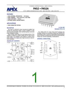
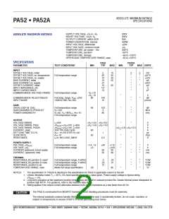
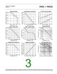
PA52 • PA52A
GENERAL
COMPENSATION
Compensation is internally fixed for a gain of 3 or more and
is not adjustable by the user. The PA52 therefore is not unity
gain stable.
Please read Application Note 1 "General Operating Con-
siderations" which covers stability, supplies, heat sinking,
mounting, current limit, SOA interpretation, and specification
interpretation. Visit www.apexmicrotech.com for design tools
that help automate tasks such as calculations for stability,
internal power dissipation, current limit; heat sink selection;
Apex’s complete Application Notes library; Technical Seminar
Workbook; and Evaluation Kits.
POWER SUPPLY BYPASSING
Proper and sufficient power supply bypassing is crucial to
proper operation of the PA52. Bypass the +Vb and -Vb supply
pins with a minimum .1µF ceramic capacitors directly at the
supply pins. On the +Vs and -Vs pins use a combination of
ceramic and electrolytic capacitors. Use 1µF ceramic capaci-
tors and an electrolytic capacitor at least 10µF for each amp
of output current required.
CURRENT LIMIT
There is no internal circuit provision for current limit in the
PA52. However, the PA52 circuit board in the PA52 evaluation
kit does provide a means whereby the output current can be
sensed. An external circuit current limit can thereby be imple-
mented if needed. See EK27 data sheet for more details.
BOOST OPERATION
With the VBOOST feature the small signal stages of the
amplifier are operated at higher supply voltages than the
amplifier’s high current output stage. +VBOOST (pin 11) and
–VBOOST (pin 12) are connected to the small signal circuitry of
the amplifier. +VS (pin 9,10) and –VS (pin 3,4) are connected to
the high current output stage. An additional 10V on the VBOOST
pins is sufficient to allow the small signal stages to drive the
outputtransistorsintosaturationandimprovetheoutputvoltage
swing for extra efficient operation when required. When close
swings to the supply rails is not required the +VBOOST and +VS
pins must be strapped together as well as the –VBOOST and –VS
pins. The boost voltage pins must not be at a voltage lower
than the VS pins.
This data sheet has been carefully checked and is believed to be reliable, however, no responsibility is assumed for possible inaccuracies or omissions. All specifications are subject to change without notice.
4APEX MICROTECHNOLOGY CORPORATION • 5980 NORTH SHANNON ROAD • TUCSON, ARIZONA 85741 • USA • APPLICATIONS HOTLINE: 1 (800) 546-2739
PA52U REV D APRIL 2003
© 2003 Apex Microtechnology Corp.

 APEX [ CIRRUS LOGIC ]