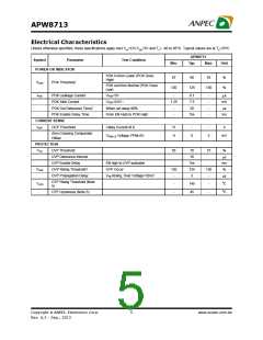
APW8713
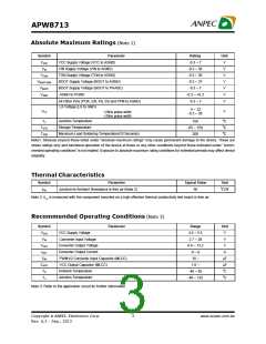
Absolute Maximum Ratings (Note 1)
Symbol
VVCC
Parameter
VCC Supply Voltage (VCC to AGND)
Rating
-0.3 ~ 7
Unit
V
VIN
VIN Supply Voltage (VIN to AGND)
TON Supply Voltage (TON to AGND)
BOOT Supply Voltage (BOOT to AGND)
BOOT Supply Voltage (BOOT to PHASE)
-0.3 ~ 30
-0.3 ~ 30
-0.3 ~ 37
-0.3 ~ 7
V
VTON
V
VBOOT-GND
VBOOT
VGND
V
V
AGND to PGND
-0.3 ~ +0.3
-0.3 ~ 7
V
All Other Pins (POK, EN, FB, SS and PFM to AGND)
LX Voltage (LX to GND)
V
-5 ~ 32
-0.3 ~ 30
VLX
V
<20ns pulse width
>20ns pulse width
TJ
150
-65 ~ 150
260
oC
oC
oC
Junction Temperature
Storage Temperature
TSTG
TSDR
Maximum Lead Soldering Temperature(10 Seconds)
Note1: Stresses beyond those listed under "absolute maximum ratings" may cause permanent damage to the device. These are
stress ratings only and functional operation of the device at these or any other conditions beyond those indicated under "recom-
mended operating conditions" is not implied. Exposure to absolute maximum rating conditions for extended periods may affect device
reliability.
Thermal Characteristics
Symbol
Parameter
Typical Value
Unit
Junction-to-Ambient Resistance in free air (Note 2)
50
oC/W
qJA
Note 2: qJA is measured with the component mounted on a high effective thermal conductivity test board in free air.
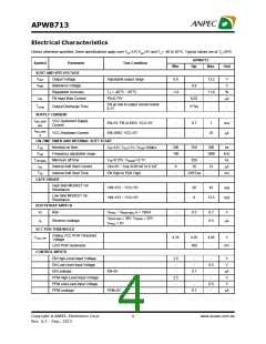
Recommended Operating Conditions (Note 3)
Symbol
VVCC
VIN
Parameter
Range
4.5 ~ 5.5
2.7 ~ 28
0.8 ~ 13.2
0 ~ 8
Unit
V
VCC Supply Voltage
Converter Input Voltage
Converter Output Voltage
Converter Output Current
V
VOUT
IOUT
CIN
V
A
PWM1/2 Converter Input Capacitor (MLCC)
VCC Output Capacitor (MLCC)
Ambient Temperature
10 ~
mF
mF
oC
oC
CVCC
TA
1.0 ~
-40 ~ 85
-40 ~ 125
Junction Temperature
TJ
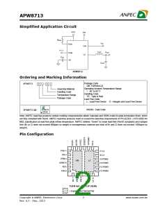
Note 3: Refer to the application circuit for further information.
Copyright ã ANPEC Electronics Corp.
3
www.anpec.com.tw
Rev. A.3 - Sep., 2013

 ANPEC [ ANPEC ELECTRONICS COROPRATION ]