APW7077/A
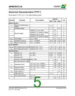
Absolute Maximum Ratings
Symbol
VDD
VIO
Parameter
Value
-0.3 to 7
Unit
V
Supply voltage
Input / output pins (CE, FB, EXT)
Operating Ambient Temperature Range
Junction Temperature Range
Storage Temperature Range
Soldering Temperature
-0.3 to 7
V
TA
-40 to 85
°C
°C
°C
°C
kV
TJ
-40 to 150
-65 to +150
300, 10 seconds
TSTG
TS
VESD
Minimum ESD Rating
±
2
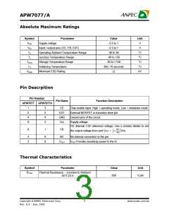
Pin Descrpition
Pin Number
Pin Name
Function Description
APW7077 APW7077A
1
5
4
X
3
5
4
2
CE
Chip enable input. High = operating mode; Low = shutdown mode
External MOSFET or transistor drive pin.
Ground pins of the circuit.
EXT
GND
DD
V
Supply voltage.
FB: Internal 1.0V reference voltage. Use a resistor divider to set
æ
R2 ö
X
1
FB
ç1+
÷
OUT
the output voltage from and V
=
÷ VFB.
R1
ç
è
ø
3
2
X
X
NC
No internal connection to the pin.
VOUT Provides bootstrap power to the IC.
VOUT
Thermal Characteristics
Symbol
Parameter
Value
Unit
-
R q
Thermal Resistance Junction to Ambient
JA
200
°
SOT-23-5
C/W
Copyright ã ANPEC Electronics Corp.
3
www.anpec.com.tw
Rev. A.4 - Sep, 2005

 ANPEC [ ANPEC ELECTRONICS COROPRATION ]