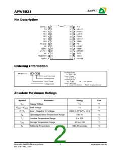
APW6021
Functional Pin Description Cont.
VID4, VID3, VID2, VID1, VID0 (Pins 3, 4, 5, 6 and 7)
SS (Pin 12)
VID0-4 are the TTL-compatible input pins to the 5-bit Connect a capacitor from this pin to ground. This
DAC. The logic states of these five pins program the capacitor, along with an internal 28µA current source,
internal voltage reference (DACOUT). The level of sets the soft-start interval of the converter.
DACOUT sets the microprocessor core converter
output voltage, as well as the corresponding PGOOD FAULT / RT (Pin 13)
and OVP thresholds.
This pin provides oscillator switching frequency
PGOOD (Pin 8)
adjustment. By placing a resistor (RT) from this pin to
GND, the nominal 200kHz switching frequency is in-
PGOOD is an open collector output used to indicate creased according to the following equation:
the status of the output voltages. This pin is pulled
low when the synchronous regulator output is not
Fs =200kHz + 5 × 10⁶ / RT (kΩ) (RT to GND)
within ±10% of the DACOUT reference voltage or
when any of the other outputs are below their under- reduces the switching frequency according to the fol-
Conversely, connecting a resistor from this pin to VCC
voltage thresholds.
lowing equation:
Fs =200kHz + 4 × 10 7 / RT (kΩ) (RT to 12V)
The PGOOD output is open for“11111” VID code.
SD (Pin 9)
Nominally, the voltage at this pin is 1.26V. In the event
of an over-voltage or over-current condition, this pin
is internally pulled to VCC.
This pin shuts down all the outputs. A TTL-
compatible, logic level high signal applied at this
pin immediately discharges the soft-start capacitor,
disabling all the outputs. Dedicated internal circuitry
insures the core output voltage does not go negative
during this process. When re-enabled, the IC under-
goes a new soft-start cycle. Left open, this pin is pulled
low by an internal pull-down resistor, enabling
operation.
VSEN4 (Pin 14)
Connect this pin to the output of the linear 1.8V
regulator. This pin is monitored for undervoltage
events.
DRIVE4 (Pin 15)
Connect this pin to the gate of an external MOSFET.
This pin provides the drive for the 1.8V regulator’s
pass transistor.
VSEN2 (Pin 10)
Connect this pin to the output of the AGP linear
regulator. The voltage at this pin is regulated to the
level predetermined by the logic-level status of the
SELECT pin. This pin is also monitored for under-
voltage events.
VAUX (Pin 16)
This pin provides boost current for the linear regula-
tors’ output drives in the event bipolar NPN transis-
tors (instead of N-channel MOSFETs) are employed
as pass elements. The voltage at this pin is moni-
tored for power-on reset (POR) purposes.
SELECT (Pin 11)
This pin determines the output voltage of the AGP
bus linear regulator. A low TTL input sets the output
voltage to 1.5V, while a high input sets the output
voltage to 3.3V.
GND (Pin 17)
Signal ground for the IC. All voltage levels are mea-
sured with respect to this pin.
Copyright ANPEC Electronics Corp.
Rev. P.4 - Mar., 2001
6
www.anpec.com.tw

 ANPEC [ ANPEC ELECTRONICS COROPRATION ]