APR3101/2/3
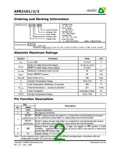
Ordering and Marking Information
Package Code
B : SOT-23-5
Temp. Range
APR3101/2/3 -
°
Lead Free Code
°
I : -40 to 85 C
Handling Code
Handling Code
TR : Tape & Reel
Voltage Code :
15 : 1.5V ~ 50 : 5.0V
Lead Free Code
L : Lead Free Device
Temp. Range
Package Code
Voltage Code
Blank : Original Device
A1/2/3 X X
APR3101/2/3 B :
Date Code
Voltage Code
A:1.5V B:1.75V C:2.32V D:2.63V E:2.93V F:3.08V G:3.9V H:4.38V
Absolute Maximum Ratings
Symbol
Parameter
Value
Unit
VCC
VCC to GND
-0.3 to 6
V
RESET to GND (Push-Pull Output)
RESET to GND (Open Drain Output)
-0.3 to VCC +0.3
-0.3 to 6
VRESET
V
ICC, IMR
IRESET
dVcc/dt
TJ
Maximum Continuous Input Current
RESET/RESET Current
20
20
mA
mA
Rate of Rise of VCC
100
V/µs
°C
Junction Temperature Range
Lead Temperature (Soldering, 10 second)
Thermal Resistance – Junction to Ambient
Power Dissipation
-40 to 150
260
TL
°C
RTH,JA
PD
357
°C/W
W
Internally Limited
-65 to +150
TSTG
Storage Temperature Range
°C
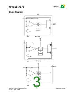
Pin Function Descrpition
PIN
Description
No.
1
Name
GND
Ground connection
2
NC
No internal connection
CC
RESET
(APR3101/3)
RESET
(APR3102)
RESET output remains low while V is below the reset threshold and remains
CC
so for a fixed time period after V raises above the reset threshold.
3
CC
RESET output remains high while V is below the reset threshold and remains
CC
so for a fixed time period after V raises above the reset threshold.
Manual Reset active low input. A logic low signal on MR asserts a reset
condition. Asserted reset continues as long as MR is low and for a fixed time
period after MR returns high.
4
5
MR
CC
V
Supply Voltage (+1.2V to +6V)
Note: The pin sequence here might not be correct for all different package types, and please refer pin
configuration in page1 for correct pin assignment.
Copyright ANPEC Electronics Corp.
Rev. A.3 - Feb., 2004
2
www.anpec.com.tw

 ANPEC [ ANPEC ELECTRONICS COROPRATION ]