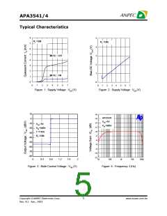
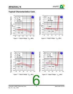
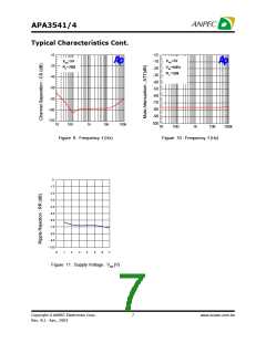
APA3541/4
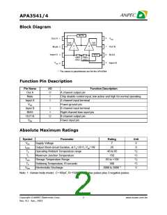
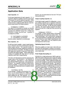
Block Diagram
MUTE
8
1
2
3
4
VDD
Out A
Mute
0dB
0dB
(6dB)
(6dB)
A
+
B
+
7
6
5
Out B
BIAS
Input B
Input A
VSS
BIAS
180kΩ
180kΩ
(90kΩ ) (90kΩ )
* The values in parenthessis are for the APA3544.
Function Pin Description
Pin Name
Out A
Mute
I/O
Function Description
O
I
A channel output pin
Chip disable control input, low active and high for normal operating
A channel input terminal
Input A
VSS
I
Power ground pin
Input B
BIAS
I
I
B channel input terminal
Right channel bias input pin
B channel output pin
OUT B
VDD
O
Power input pin
Absolute Maximum Ratings
Symbol
VDD
Parameter
Rating
Unit
V
Supply Voltage
7
20
tSC(O)
TA
S
Output Short-circuit Duration, at T =25 C, P =1W
°
A
tot
Operating Ambient Temperature range
-40 to 85
150
C
°
C
°
C
°
C
°
TJ
Maximum Junction Temperature
Storage Temperature Range
Soldering Temperature,10 seconds
Electrostatic Discharge
TSTG
TS
-65 to +150
300
-3000 to 3000 *1
VESD
V
Note: 1. Human body model : C=100pF, R=1500Ω, 3 positive pulses plus 3 negative pulses
Copyright ANPEC Electronics Corp.
Rev. B.1 -Apr., 2003
2
www.anpec.com.tw

 ANPEC [ ANPEC ELECTRONICS COROPRATION ]