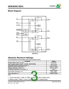
APA2030/2031
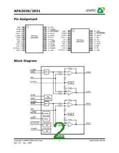
Pin Descriptions
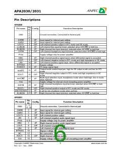
APA2030
Pin
Pin name
Config.
Function Description
no.
1,
12,
13,
24
2
GND
-
Ground connection, Connected to thermal pad.
GAIN0
GAIN1
LOUT+
LLINEIN
RLINEIN
LHPIN
I/P
I/P
Input signal for internal gain setting
Input signal for internal gain setting
Left channel positive output in BTL mode and SE mode
Left channel line input terminal, selected when HP/LINE is held low.
Right channel line input terminal, selected when HP/LINE is held low.
Left channel headphone input terminal, selected when HP/LINE is held high.
3
4
O/P
I/P
5
23
I/P
6
7,
18
8
O/P
PVDD
-
Supply voltage only for power amplifier
RIN+
LOUT-
LIN+
BYPASS
PCBEEP
I/P
O/P
I/P
-
Right channel positive signal input, when differential signal is accepted.
Left channel negative output in BTL mode and high impedance in SE mode
Left channel positive signal input, when differential signal is accepted.
9
10
11
14
Bypass voltage
I/P
PC-beep signal input
Output mode control input pin, high for SE output mode and low for BTL
15
I/P
SE/BTL
ROUT-
mode
Right channel negative output in BTL mode and high impedance in SE
16
O/P
mode
Multi-input selection input, headphone mode when held high, line-in mode
HP/LINE
VDD
17
19
20
I/P
-
when held low
Supply voltage for internal circuit excepting power amplifier.
Right channel headphone input terminal, selected when HP/LINE is held
high.
Right channel positive output in BTL mode and SE mode
It will be into shutdown mode when pull low
Right channel line input terminal, selected when HP/LINE is held low
RHPIN
ROUT+
SHUTDOW N
RLINEIN
I/P
21
22
23
O/P
I/P
I/P
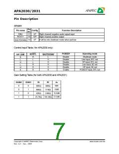
APA2031
Pin name
Pin
no.
Config.
Function Description
1, 11,
13, 20
2
GND
-
Ground connection, Connected to thermal pad.
GAIN0
GAIN1
LOUT+
LIN-
PVDD
RIN+
LOUT-
LIN+
BYPASS
NC
ROUT-
VDD
I/P
I/P
O/P
I/P
-
Input signal for internal gain setting
Input signal for internal gain setting
Left channel positive output
Left channel negative audio signal input
Supply voltage only for power amplifier
Right channel positive audio signal input
Left channel negative output
Left channel positive audio signal input
Bypass voltage
3
4
5
6,15
7
8
9
10
12
14
16
I/P
O/P
I/P
-
-
No connection
O/P
-
Right channel negative output
Supply voltage for internal circuit excepting power amplifier
Copyright ANPEC Electronics Corp.
6
www.anpec.com.tw
Rev. A.2 - Apr., 2004

 ANPEC [ ANPEC ELECTRONICS COROPRATION ]