Model XC0450A-03
Rev B
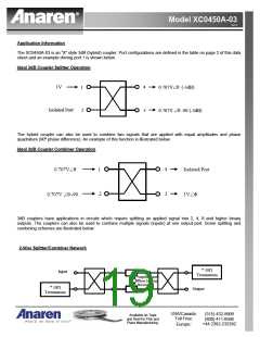
Signal Control Circuits Utilizing 3dB Couplers
Variable attenuators and phase shifter are two examples of signal control circuits that can be built using 3dB couplers.
Both of these circuits also use the reflection property of the 3dB coupler as described above. In the variable attenuator
circuit, the two output ports of a 3dB coupler are terminated with PIN diodes, which are basically a voltage variable
resistor at RF frequencies (consult the literature on PIN diodes for a more complete equivalent circuit). By changing the
resistance at the output ports of the 3dB coupler, the reflection coefficient, Γ, will also change and different amounts of
energy will be reflected to the isolated port (note that the resistances must change together so that Γ is the same for
both output ports). A signal applied to the input of the 3dB coupler will appear at the isolated port and the amplitude of
this signal will be a function of the resistance at the output ports. This circuit is illustrated below:
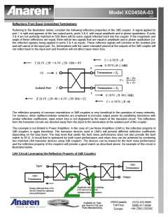
Variable Attenuator Circuit Utilizing a 3dB Coupler
Γ× 0.707V ∠θ
0.707V∠θ (-3dB)
4
Input
1
PIN Diodes
Vdc
Output
2
3
0.707V ∠θ -90 (-3dB)
Γ× 0.707V ∠θ -90
|Γ (0.5V ∠2θ -90 + 0.5V ∠2θ -90)| = |Γ|
and
If Γ=0, no energy is reflected from the PIN diodes and S21 = 0 (input to output). If | Γ | =1, all of the energy is reflected
from the PIN diodes and |S21| = 1 (assuming the ideal case of no loss). The ideal range for Γ is –1 to 0 or 0 to 1, which
translate to resistances of 0ꢀ to 50ꢀ and 50ꢀ to ∞ꢀ respectively. Either range can be selected, although normally 0ꢀ
to 50ꢀ is easier to achieve in practice and produces better results. Many papers have been written on this circuit and
should be consulted for the details of design and operation.
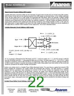
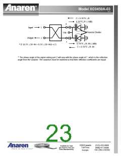
Another very similar circuit is a Variable Phase Shifter (illustrated below). The same theory is applied but instead of PIN
diodes (variable RF resistance), the coupler outputs are terminated with varactors. The ideal varactor is a variable
capacitor with the capacitance value changing as a function of the DC bias. Ideally, the magnitude of the reflection
coefficient is 1 for these devices at all bias levels. However, the angle of the reflected signal does change as the
capacitance changes with bias level. So, ideally all of the energy applied to port 1, in the circuit illustrated below, will be
reflected at the varactors and will sum at port 2 (the isolated port of the coupler). However, the phase angle of the signal
will be variable with the DC bias level. In practice, neither the varactors nor the coupler are ideal and both will have
some losses. Again, many papers have been written on this circuit and should be consulted for the details of design and
operation.
Variable Phase Shifter Circuit Utilizing a 3dB Coupler
USA/Canada:
Toll Free:
Europe:
(315) 432-8909
(800) 411-6596
+44 2392-232392
Available on Tape and
Reel for Pick and Place
Manufacturing.

 ANAREN [ ANAREN MICROWAVE ]