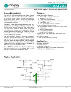
PRODUCT DATASHEET
AAT2550178
SystemPowerTM
Total Power Solution for Portable Applications
Pin Descriptions
Pin #
Symbol Function
Enable pin for Converter A. When connected to logic low, it disables the step-down converter and con-
sumes less than 1μA of current. When connected to logic high, the converter operates normally.
Power switching node for Converter A. Connect the inductor to this pin. Internally, it is connected to the
drain of both high- and low-side MOSFETs.
1
ENA
LXA
2
Power ground. Connect the PGND pins together as close to the IC as possible. Connect AGND to PGND at a
single point as close to the IC as possible.
3, 17
PGND
4
5, 7
DATA
N/C
Status report to the microcontroller via serial interface (open drain).
Not connected.
Charge current set point. Connect a resistor from this pin to ground. Refer to Typical Characteristics curves
for resistor selection.
6
ADPSET
8
9
BAT
ADP
Battery charging and sensing. Connect the positive terminal of the battery to BAT.
Input for adapter charger.
10, 11, 22
AGND
Analog signal ground. Connect AGND to PGND at a single point as close to the IC as possible.
Enable pin for the battery charger. When connected to logic low, the battery charger is disabled and con-
sumes less than 1μA of current. When connected to logic high, the charger operates normally.
12
ENBAT
13
14
15
TS
STAT2
STAT1
Temperature sense input. Connect to a 10kΩ NTC thermistor.
Battery charge status indicator pin to drive an LED. It is an open drain input.
Battery charge status indicator pin to drive an LED. It is an open drain input.
Timing capacitor to adjust internal watchdog timer. Sets maximum charge time for adapter powered
trickle, constant current, and constant voltage charge modes.
Power switching node for Converter B. Connect the inductor to this pin. Internally, it is connected to the
drain of both high- and low-side MOSFETs.
16
18
CT
LXB
Enable pin for Converter B. When connected to logic low, it disables the step-down converter and con-
sumes less than 1μA of current. When connected to logic high, the converter operates normally.
Input voltage for Converter B.
Output voltage feedback input for Converter B. FBB senses the output voltage B for regulation control. The
FBB regulation threshold is 0.6V. A resistive voltage divider is connected to the output B, FBB, and AGND.
19
20
21
ENB
INB
FBB
Output voltage feedback input for Converter A. FBA senses the output voltage A for regulation control. The
FBA regulation threshold is 0.6V. A resistive voltage divider is connected to the output A, FBA, and AGND.
Input voltage for Converter A.
23
FBA
INA
24
EP
Exposed paddle; connect to ground directly beneath the package.
Pin Configuration
QFN44-24
(Top View)
1
2
3
4
5
6
18
17
16
15
14
13
LXB
PGND
CT
STAT1
STAT2
TS
ENA
LXA
PGND
DATA
N/C
ADPSET
w w w . a n a l o g i c t e c h . c o m
2
2550.2008.02.1.3

 ANALOGICTECH [ ADVANCED ANALOGIC TECHNOLOGIES ]