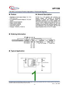
AP1186
1.5A Ultra Low Dropout Positive Adjustable or Fixed-mode Regulator
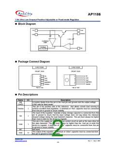
Block Diagram
Vin
Vout
Vsense
Vctrl
+
+
+
1.25V
+
-
CURRENT
LIMIT
THERMAL
Adj
SHUTDOWN
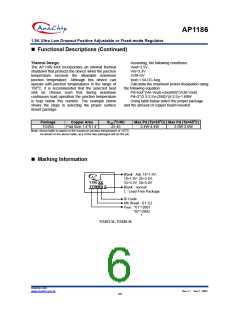
Package Connect Diagram
5 PIN TO263
FRONT VIEW
5 PIN TO220
FRONT VIEW
Vin
Vctrl
Vout
Adj(GND)
Vsense
5
4
3
2
1
Vin
Vctrl
Vout
Adj(GND)
Vsense
5
4
3
2
1
Tab is Vout
Tab is Vout
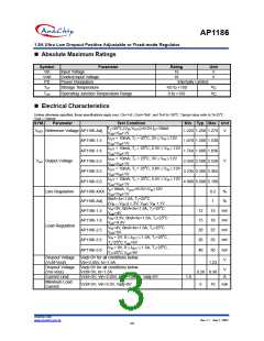
Pin Descriptions
Name
Adj
I/O
Description
A resistor divider from this pin to the Vout pin and ground sets the output voltage.
(GND only for fixed mode)
(GND)
This pin is the positive side of the reference that allows remote load sensing to
achieve excellent load regulation. A minimum of 10uF capacitor must be connected
from this pin to ground to insure stability.
The input of the regulator. Typically a large storage capacitor is connected from this
pin to ground to insure that the input voltage does not sag below the minimum
dropout voltage during the load transient response. This pin must always be higher
than Vout in order for the device to regulate.
Vsense
Vin
I
I
This pin is the supply pin for the internal control circuit as well as the base drive for
the pass transistor. This pin must always by higher than the Vout pin in order the
device to regulate. A minimum of 100uF capacitor must be connected from this pin
to ground to insure stability.
Vctrl
I
NC
Not used.
The output of the regulator. A minimum of 100uF capacitor must be connected from
this pin to ground to insure stability.
Vout
O
Anachip Corp.
www.anachip.com.tw
Rev.1.1 Sep.7, 2004
2/8

 ANACHIP [ ANACHIP CORP ]