AS13985
Datasheet - Absolute Maximum Ratings
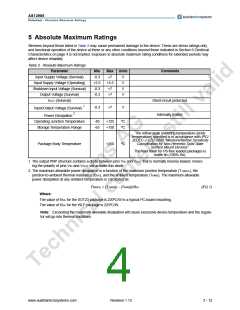
5 Absolute Maximum Ratings
Stresses beyond those listed in Table 2 may cause permanent damage to the device. These are stress ratings only,
and functional operation of the device at these or any other conditions beyond those indicated in Section 6 Electrical
Characteristics on page 4 is not implied. Exposure to absolute maximum rating conditions for extended periods may
affect device reliability.
Table 2. Absolute Maximum Ratings
Parameter
Min
-0.3
+2.5
-0.3
-0.3
Max Units
Comments
Input Supply Voltage (Survival)
Input Supply Voltage (Operating)
Shutdown Input Voltage (Survival)
Output Voltage (Survival)
IOUT (Survival)
+7
+5.5
+7
V
V
V
V
+7
Short-circuit protected.
Internally limited.
Input/Output Voltage (Survival) 1
-0.3
+7
V
Power Dissipation 2
Operating Junction Temperature
Storage Temperature Range
-40
-65
+125
+150
ºC
ºC
The reflow peak soldering temperature (body
temperature) specified is in accordance with IPC/
JEDEC J-STD-020D “Moisture/Reflow Sensitivity
Classification for Non-Hermetic Solid State
Surface Mount Devices”.
Package Body Temperature
+260
ºC
The lead finish for Pb-free leaded packages is
matte tin (100% Sn).
1. The output PNP structure contains a diode between pins VIN and VOUT that is normally reverse-biased. revers-
ing the polarity of pins VIN and VOUT will activate this diode.
2. The maximum allowable power dissipation is a function of the maximum junction temperature (TJ(MAX), the
junction-to-ambient thermal resistance (ΘJA), and the ambient temperature (TAMB). The maximum allowable
power dissipation at any ambient temperature is calculated as:
P(MAX) = (TJ(MAX) - (TAMB))/ΘJA
(EQ 1)
Where:
The value of ΘJA for the SOT23 package is 220ºC/W in a typical PC-board mounting.
The value of ΘJA for the WLP package is 225ºC/W.
Note: Exceeding the maximum allowable dissipation will cause excessive device temperature and the regula-
tor will go into thermal shutdown.
www.austriamicrosystems.com
Revision 1.13
3 - 12

 AMSCO [ AMS(艾迈斯) ]