AMD
FUNCTIONAL DESCRIPTION
Standard 20-Pin PAL Family
Registers with Feedback
Registered outputs are provided for data storage and
synchronization. Registers are composed of D-type
flip-flops that are loaded on the LOW-to-HIGH transition
of the clock input.
The standard bipolar 20-pin PAL family devices have
common electrical characteristics and programming
procedures. Four different devices are available, includ-
ing both registered and combinatorial devices. All parts
are produced with a fuse link at each input to the AND
gate array, and connections may be selectively re-
moved by applying appropriate voltages to the circuit.
Utilizing an easily-implemented programming algo-
rithm, these products can be rapidly programmed to
any customized pattern. Extra test words are pre-
programmed during manufacturing to ensure extremely
high field programming yields, and provide extra test
paths to achieve excellent parametric correlation.
Register Preload
TheregisterontheAMDmarked16R8, 16R6, and16R4
devices can be preloaded from the output pins to facili-
tate functional testing of complex state machine de-
signs. This feature allows direct loading of arbitrary
states, making it unnecessary to cycle through long test
vector sequences to reach a desired state. In addition,
transitions from illegal states can be verified by loading
illegal states and observing proper recovery.
Power-Up Reset
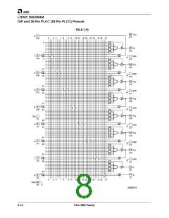
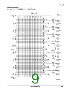
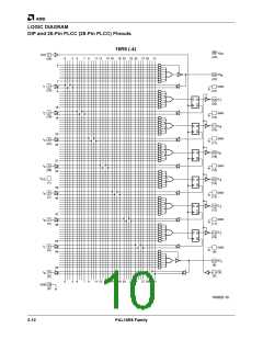
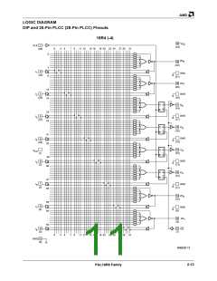
Pinouts
All flip-flops power-up to a logic LOW for predictable
system initialization. Outputs of the PAL16R8 Family
will be HIGH due to the active-low outputs. The VCC rise
must be monotonic and the reset delay time is 1000 ns
maximum.
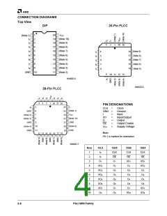
The PAL16R8 Family is available in the standard 20-pin
DIP and PLCC pinouts and the PAL16R8-4 Series is
available in the new 28-pin PLCC pinout. The 28-pin
PLCC pinout gives the designer the cleanest possible
signal with only 4.5 ns delay.
The PAL16R8-4 pinout has been designed to minimize
the noise that can be generated by high-speed signals.
Because of its inherently shorter leads, the PLCC pack-
age is the best package for use in high-speed designs.
The short leads and multiple ground signals reduce the
effective lead inductance, minimizing ground bounce.
Placing the ground pins between the outputs optimizes
the ground bounce protection, and also isolates the out-
puts from each other, eliminating cross-talk. This pinout
can reduce the effective propagation delay by as much
as 20% from a standard DIP pinout. Design files for
PAL16R8-4 Series devices are written as if the device
had a standard 20-pin DIP pinout for most design soft-
ware packages.
Security Fuse
After programming and verification, a PAL16R8 Family
design can be secured by programming the security
fuse. Once programmed, this fuse defeats readback of
the internal programmed pattern by a device program-
mer, securing proprietary designs from competitors.
When the security fuse is programmed, the array will
read as if every fuse is programmed.
Quality and Testability
The PAL16R8 Family offers a very high level of built-in
quality. Extra programmable fuses provide a means of
verifying performance of all AC and DC parameters. In
addition, this verifies complete programmability and
functionality of the device to provide the highest pro-
gramming yields and post-programming functional
yields in the industry.
Variable Input/Output Pin Ratio
The registered devices have eight dedicated input lines,
and each combinatorial output is an I/O pin. The
PAL16L8 has ten dedicated input lines and six of the
eight combinatorial outputs are I/O pins. Buffers for de-
vice inputs have complementary outputs to provide
user-programmable input signal polarity. Unused input
pins should be tied to VCC or GND.
Technology
The PAL16R8-5, -7 and D/2 are fabricated with AMD’s
oxide isolated bipolar process. The array connections
are formed with highly reliable PtSi fuses. The
PAL16R8B, B-2, A and B-4 series are fabricated with
AMD’s advanced trench-isolated bipolar process. The
array connections are formed with proven TiW fuses for
reliable operation. These processes reduce parasitic
capacitances and minimum geometries to provide
higher performance.
Programmable Three-State Outputs
Each output has a three-state output buffer with three-
state control. On combinatorial outputs, a product term
controls the buffer, allowing enable and disable to be a
function of any product of device inputs or output feed-
back. The combinatorial output provides a bidirectional
I/O pin and may be configured as a dedicated input if the
output buffer is always disabled. On registered outputs,
an input pin controls the enabling of the three-state
outputs.
2-9
PAL16R8 Family

 AMD [ AMD ]