AMD
P R E L I M I N A R Y
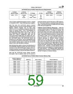
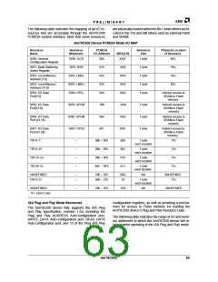
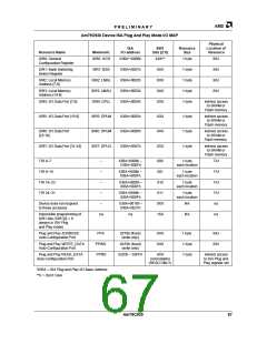
The following table indicates the mapping of all I/O re-
sources that are accessible through the Am79C930
PCMCIA system interface. Note that some resources
are physically located within the BIU, while others are lo-
cated in the TAI and still others exist as external Flash
and SRAM:
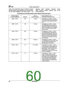
Am79C930 Device PCMCIA Mode I/O MAP
Resource
Name
Resource
Mnemonic
PCMCIA
I/O Address
Resource
Physical Location
of Resource
SIR1[2:0]
Size
SIR0: General
Configuration Register
SIR0: GCR
00h
01h
02h
03h
04h
XXX*
1 byte
BIU
BIU
BIU
BIU
SIR1: Bank Switching
Select Register
SIR1: BSS
SIR2: LMAL
SIR3: LMAU
SIR4: DPLL
XXX
XXX
XXX
XXX
1 byte
1 byte
1 byte
1 byte
SIR2: Local Memory
Address [7:0]
SIR3: Local Memory
Address [14:8]
SIR4: I/O Data
Port[7:0]
Indirect access to
SRAM or Flash
memory
SIR5: I/O Data
Port[15:8]
SIR5: DPLM
SIR6: DPUM
SIR7: DPUU
05h
06h
07h
XXX
XXX
XXX
1 byte
1 byte
1 byte
Indirect access to
SRAM or Flash
memory
SIR6: I/O Data
Port [23:16]
Indirect access to
SRAM or Flash
memory
SIR7: I/O Data
Port [31:24]
Indirect access to
SRAM or Flash
memory
TIR 0–7
–
–
–
–
08h – 0Fh
08h – 0Fh
08h – 0Fh
08h – 0Fh
000
001
010
011
1 byte
each location
TAI
TAI
TAI
TAI
TIR 8–15
TIR 16–23
TIR 24–31
1 byte
each location
1 byte
each location
1 byte
each location
UNDEFINED
TIR 0–31
–
–
10h – 3Fh
08h – 27h
0XX
1X
NA
UNDEFINED
TAI
1 byte
each location
UNDEFINED
–
28h – 3Fh
1XX
NA
UNDEFINED
*X = Don’t Care
ISA Plug and Play Mode Resources
configuration registers, as well as providing a mecha-
nism for access to Flash memory for reading the
Am79C930 device’s Plug and Play Resource Data.
The Am79C930 device fully supports the ISA Plug
and Play specification, revision 1.0a, including the
Plug and Play ADDRESS Auto-configuration port,
WRITE_DATA Auto-configuration port, READ_DATA
Auto-configuration port, and 19 of the Plug and Play
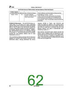
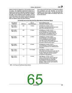
The following table indicates the range of I/O and mem-
ory addresses to which the Am79C930 device will re-
spond when operating in the ISA Plug and Play mode.
Am79C930
63

 AMD [ AMD ]