AMD
P R E L I M I N A R Y
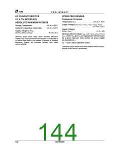
AC CHARACTERISTICS
OPERATING RANGES
Commercial (C) Devices
5.0 AND 3.3 V USER
Temperature (TA) . . . . . . . . . . . . . . . . . 0°C to + 70°C
PROGRAMMABLE PINS
Supply Voltages (VCC,VDDT, VDDU1, VDDU2, VDDM, VDDP)
. . . . . . . . . . . . . . . . . . . . . . . . . . . . . . 3.0 V to 5.25 V
ABSOLUTE MAXIMUM RATINGS
Storage Temperature: . . . . . . . . . . . . –65 to +150°C
Ambient Temperature Under Bias: . . . –65 to +125°C
Supply Voltages
(AVDD, VDD5) . . . . . . . . . . . . . . . . . . . . . . . . +5 V ± 5%
Supply Voltage to AVSS
or DVSS (AVDD, DVDD): . . . . . . . . . . . . . . –0.3 to +6 V
All inputs within the range: VSS – 0.5 V≤ VIN ≤ VDD + 0.1 X
VDD – where VSS and VDD are appropriate reference pins
for a given input pin. (See section on power supply
pin descriptions.)
Stresses above those listed under Absolute Maximum
Ratings may cause permanent device failure. Functionality at
or above these limits is not implied. Exposure to Absolute
Maximum Ratings for extended periods may affect
device reliability.
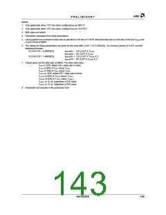
CL = 50 pF unless otherwise noted
Operating ranges define those limits between which the func-
tionality of the device is guaranteed.
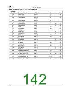
Parameter
Symbol
Parameter Description
Test Conditions
Min
Max
Units
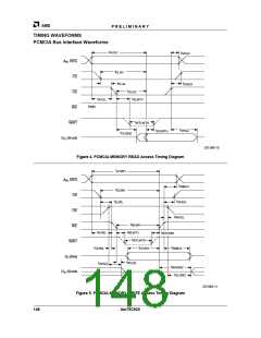
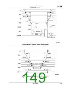
tu1
Data change delay from
55
ns
CLKIN ↓
tu2
tu3
Pin drive disable delay from
CLKIN ↓
55
55
ns
ns
Note 1
Note 1
Pin drive enable delay from
CLKIN ↓
Note:
1. Parameter is not included in production test.
146
Am79C930

 AMD [ AMD ]