Revision 1.02 – June 27, 2006
S5935 – PCI Product
Data Book
Signal
ERD#/SCL
Type
Direction
Max
1
Units
mA
Notes
Output
Bi-directional
EWR#/SDA
t/s
1
mA
AC CHARACTERISTICS
PCI Bus Timings
Functional Operation Range (V CC =5.0V ±5%, 0°C to 70°C, 50 pF load on outputs)
Symbol
Parameter
Min
30
Max
Units
ns
Notes
TCL
t1
Cycle Time
High Time
Low Time
12
ns
t2
12
ns
t3
Rise Time (0.8V to 2.0V)
Fall Time (2.0V to 0.8V)
3
3
ns
t4
ns
t5
Output Valid Delay (Bussed Signals)
Output Valid Delay (Point-to-Point Signals)
2
2
11
12
ns
Note 1
t6
t7
t8
Float to Active Delay
Active to Float Delay
2
ns
ns
28
ns
Rising Edge Setup (Bussed Signals)
Rising Edge Setup (GNT#)
Rising Edge Setup (REQ#)
7
10
12
t9
Hold from PCI Clock Rising Edge
PCICLK to BPCLK Delay
0
2
ns
ns
t10
6.5
Note:
1. Minimum times are for unloaded outputs, maximum times are for 50 pF equivalent loads.
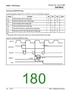
Figure 91. PCI Clock Timing
t
t
t
3
4
1
V
IH2
2.0
2.0
0.8
2.0
0.8
2.0
0.8
t
2
TCL
176
DS1527
AMCC Confidential and Proprietary

 AMCC [ APPLIED MICRO CIRCUITS CORPORATION ]