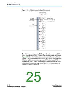
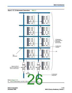
MAX II Architecture
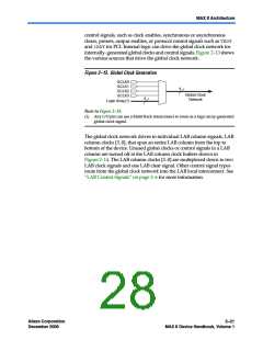
control signals, such as clock enables, synchronous or asynchronous
clears, presets, output enables, or protocol control signals such as TRDY
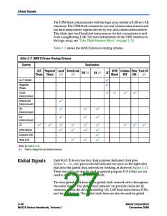
and IRDYfor PCI. Internal logic can drive the global clock network for
internally- generated global clocks and control signals. Figure 2–13 shows
the various sources that drive the global clock network.
Figure 2–13. Global Clock Generation
GCLK0
GCLK1
GCLK2
4
Global Clock
Network
GCLK3
4
Logic Array(1)
Note to Figure 2–13:
(1) Any I/O pin can use a MultiTrack interconnect to route as a logic array-generated
global clock signal.
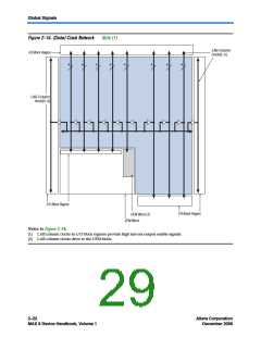
The global clock network drives to individual LAB column signals, LAB
column clocks [3..0], that span an entire LAB column from the top to
bottom of the device. Unused global clocks or control signals in a LAB
column are turned off at the LAB column clock buffers shown in
Figure 2–14. The LAB column clocks [3..0] are multiplexed down to two
LAB clock signals and one LAB clear signal. Other control signal types
route from the global clock network into the LAB local interconnect. See
“LAB Control Signals” on page 2–6 for more information.
Altera Corporation
December 2006
Core Version a.b.c variable
2–21
MAX II Device Handbook, Volume 1

 ALTERA [ ALTERA CORPORATION ]