Chapter 1: Cyclone IV Device Datasheet
1–31
Switching Characteristics
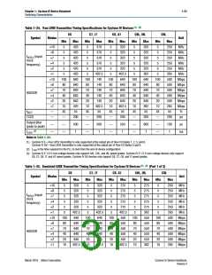
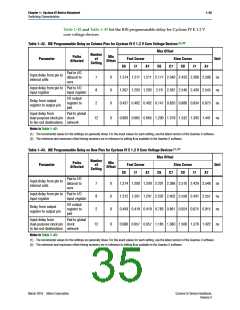
Table 1–34. True LVDS Transmitter Timing Specifications for Cyclone IV Devices (1), (3)
C6
C7, I7
Min
C8, A7
Min
C8L, I8L
Min
C9L
Symbol
Modes
Unit
Min
5
Max
420
420
420
420
420
420
840
840
840
840
840
420
55
Max
370
370
370
370
370
402.5
740
740
740
740
740
402.5
55
Max
320
320
320
320
320
402.5
640
640
640
640
640
402.5
55
Max
320
320
320
320
320
362
640
640
640
640
640
362
55
Min
5
Max
250
250
250
250
250
265
500
500
500
500
500
265
55
×10
×8
×7
×4
×2
×1
×10
×8
×7
×4
×2
×1
—
—
5
5
5
5
5
5
MHz
MHz
MHz
MHz
MHz
MHz
Mbps
Mbps
Mbps
Mbps
Mbps
Mbps
%
5
5
f
HSCLK (input
clock
frequency)
5
5
5
5
5
5
5
5
5
5
5
5
5
5
5
5
5
5
5
5
100
80
70
40
20
10
45
—
100
80
70
40
20
10
45
—
100
80
70
40
20
10
45
—
100
80
70
40
20
10
45
—
100
80
70
40
20
10
45
—
HSIODR
tDUTY
TCCS
200
200
200
200
200
ps
Output jitter
(peak to peak)
—
—
—
500
1
—
—
500
1
—
—
550
1
—
—
600
1
—
—
700
1
ps
(2)
tLOCK
—
ms
Notes to Table 1–34:
(1) Cyclone IV E—true LVDS transmitter is only supported at the output pin of Row I/O Banks 1, 2, 5, and 6.
Cyclone IV GX—true LVDS transmitter is only supported at the output pin of Row I/O Banks 5 and 6.
(2) tLOCK is the time required for the PLL to lock from the end-of-device configuration.
(3) Cyclone IV E 1.0 V core voltage devices only support C8L, C9L, and I8L speed grades. Cyclone IV E 1.2 V core voltage devices only support
C6, C7, C8, I7, and A7 speed grades. Cyclone IV GX devices only support C6, C7, C8, and I7 speed grades.
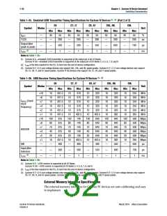
Table 1–35. Emulated LVDS Transmitter Timing Specifications for Cyclone IV Devices (1), (3) (Part 1 of 2)
C6
C7, I7
C8, A7
C8L, I8L
Min
C9L
Symbol
Modes
Unit
Min
5
Max
320
Min
Max
320
Min
Max
275
Max
275
275
275
275
275
362
550
550
550
550
550
362
Min
5
Max
250
250
250
250
250
265
500
500
500
500
500
265
×10
×8
×7
×4
×2
×1
×10
×8
×7
×4
×2
×1
5
5
5
5
5
5
MHz
MHz
5
320
320
275
5
f
HSCLK (input
clock
frequency)
5
320
5
320
5
275
5
5
MHz
5
320
5
320
5
275
5
5
MHz
5
320
5
320
5
275
5
5
MHz
5
402.5
640
5
402.5
640
5
402.5
550
5
5
MHz
100
80
70
40
20
10
100
80
70
40
20
10
100
80
70
40
20
10
100
80
70
40
20
10
100
80
70
40
20
10
Mbps
Mbps
Mbps
Mbps
Mbps
Mbps
640
640
550
640
640
550
HSIODR
640
640
550
640
640
550
402.5
402.5
402.5
March 2016 Altera Corporation
Cyclone IV Device Handbook,
Volume 3

 ALTERA [ ALTERA CORPORATION ]