Timing Model
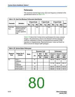
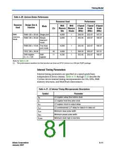
Table 4–20. Cyclone Device Performance
Resources Used
M4K
Performance
-6 Speed -7 Speed -8 Speed
Resource
Used
Design Size &
Function
M4K
Mode
LEs
Memory Memory
Grade
(MHz)
Grade
(MHz)
Grade
(MHz)
Bits
Blocks
M4K
memory
block
RAM 128 × 36 bit Single port
-
-
4,608
4,608
1
1
256.00
255.95
222.67
222.67
197.01
196.97
RAM 128 × 36 bit Simple
dual-port
mode
RAM 256 × 18 bit True dual-
port mode
-
4,608
1
255.95
222.67
196.97
FIFO 128 × 36 bit
-
40
11
4,608
4,536
1
1
256.02
255.95
222.67
222.67
197.01
196.97
Shift register
9 × 4 × 128
Shift
register
Note to Table 4–20:
(1) The performance numbers for this function are from an EP1C6 device in a 240-pin PQFP package.
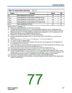
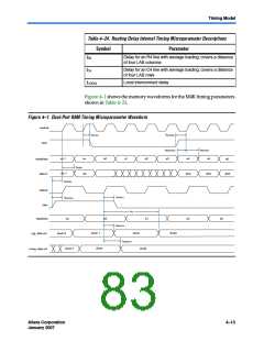
Internal Timing Parameters
Internal timing parameters are specified on a speed grade basis
independent of device density. Tables 4–21 through 4–24 describe the
Cyclone device internal timing microparameters for LEs, IOEs, M4K
memory structures, and MultiTrack interconnects.
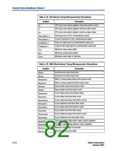
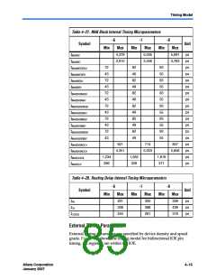
Table 4–21. LE Internal Timing Microparameter Descriptions
Symbol
Parameter
LE register setup time before clock
LE register hold time after clock
LE register clock-to-output delay
LE combinatorial LUT delay for data-in to data-out
Minimum clear pulse width
tSU
tH
tCO
tLUT
tCLR
tPRE
Minimum preset pulse width
tCLKHL
Minimum clock high or low time
Altera Corporation
January 2007
4–11
Preliminary

 ALTERA [ ALTERA CORPORATION ]