DC and Switching Characteristics
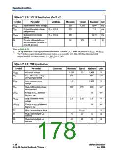
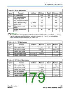
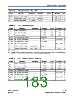
Table 4–23. LVPECL Specifications
Symbol
VCCIO (1)
VID
Parameter
Conditions
Minimum
3.135
Typical
3.3
Maximum Unit
I/O supply voltage
3.465
1,000
V
Input differential voltage
swing (single-ended)
300
600
mV
VICM
VOD
Input common mode voltage
1.0
2.5
V
Output differential voltage
(single-ended)
RL = 100 Ω
RL = 100 Ω
525
970
mV
VOCM
RL
Output common mode
voltage
1,650
90
2,250
110
mV
Receiver differential input
resistor
100
Ω
Note to Table 4–23:
(1) The top and bottom clock input differential buffers in I/O banks 3, 4, 7, and 8 are powered by VCCINT, not VCCIO
The PLL clock output/feedback differential buffers are powered by VCC_PLL_OUT. For differential clock
output/feedback operation, connect VCC_PLL_OUTto 3.3 V.
.
Table 4–24. 3.3-V PCI Specifications
Symbol
VCCIO
VIH
Parameter
Conditions
Minimum
3.0
Typical
Maximum Unit
Output supply voltage
High-level input voltage
Low-level input voltage
High-level output voltage
Low-level output voltage
3.3
3.6
V
V
V
V
V
0.5 VCCIO
–0.3
VCCIO + 0.5
0.3 VCCIO
VIL
VOH
IOUT = –500 μA
IOUT = 1,500 μA
0.9 VCCIO
VOL
0.1 VCCIO
Table 4–25. PCI-X Mode 1 Specifications
Symbol
VCCIO
VIH
Parameter
Output supply voltage
High-level input voltage
Low-level input voltage
Input pull-up voltage
Conditions
Minimum
3.0
Typical
Maximum Unit
3.6
V
V
V
V
V
V
0.5 VCCIO
–0.3
VCCIO + 0.5
0.35 VCCIO
VIL
VIPU
0.7 VCCIO
0.9 VCCIO
VOH
High-level output voltage
Low-level output voltage
IOUT = –500 μA
IOUT = 1,500 μA
VOL
0.1 VCCIO
Altera Corporation
May 2008
4–25
Arria GX Device Handbook, Volume 1

 ALTERA [ ALTERA CORPORATION ]