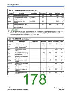
Operating Conditions
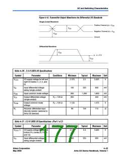
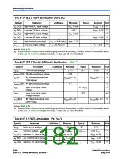
Table 4–21. 3.3-V LVDS I/O Specifications (Part 2 of 2)
Symbol
Parameter
Conditions
Minimum
200
Typical
Maximum Unit
VICM
Input common mode voltage
1,250
1,800
710
mV
mV
VOD
VOCM
RL
Output differential voltage
(single-ended)
RL = 100 Ω
RL = 100 Ω
250
Output common mode
voltage
840
90
1,570
110
mV
Receiver differential input
discrete resistor (external to
Arria GX devices)
100
Ω
Note to Table 4–21:
(1) The top and bottom clock input differential buffers in I/O banks 3, 4, 7, and 8 are powered by VCCINT, not VCCIO
The PLL clock output/feedback differential buffers are powered by VCC_PLL_OUT. For differential clock
output/feedback operation, connect VCC_PLL_OUTto 3.3 V.
.
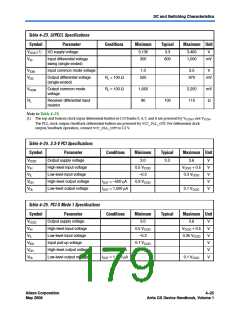
Table 4–22. 3.3-V PCML Specifications
Symbol
Parameter
Conditions
Minimum Typical Maximum Units
VCCIO
I/O supply voltage
3.135
300
3.3
3.465
600
V
VID
Input differential voltage
swing (single-ended)
mV
VICM
VOD
Input common mode
voltage
1.5
3.465
500
50
V
Output differential voltage
(single-ended)
300
370
mV
mV
V
ΔVOD
VOCM
ΔVOCM
Change in VOD between
high and low
Output common mode
voltage
2.5
2.85
3.3
Change in VOCM between
high and low
50
mV
VT
R1
Output termination voltage
VCCIO
50
V
Output external pull-up
resistors
45
45
55
55
Ω
R2
Output external pull-up
resistors
50
Ω
4–24
Altera Corporation
May 2008
Arria GX Device Handbook, Volume 1

 ALTERA [ ALTERA CORPORATION ]