DC and Switching Characteristics
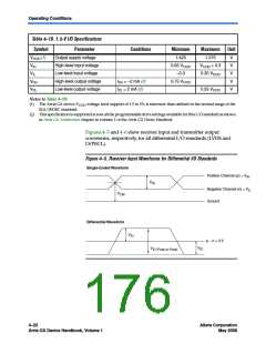
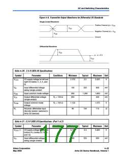
Figure 4–6. Transmitter Output Waveforms for Differential I/O Standards
Single-Ended Waveform
Positive Channel (p) = V
OH
V
OD
Negative Channel (n) = V
OL
V
CM
Ground
Differential Waveform
V
OD
p − n = 0 V
V
OD
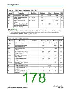
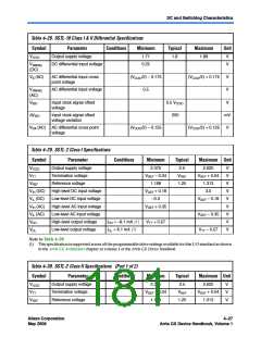
Table 4–20. 2.5-V LVDS I/O Specifications
Symbol
Parameter
Conditions
Minimum
Typical
Maximum Unit
VCCIO
I/O supply voltage for left and
right I/O banks (1, 2, 5, and
6)
2.375
2.5
2.625
V
VID
Input differential voltage
swing (single-ended)
100
350
900
mV
VICM
VOD
Input common mode voltage
200
250
1,250
1,800
450
mV
mV
Output differential voltage
(single-ended)
RL = 100 Ω
RL = 100 Ω
VOCM
RL
Output common mode
voltage
1.125
90
1.375
110
V
Receiver differential input
discrete resistor (external to
Arria GX devices)
100
Ω
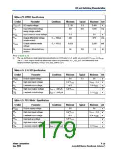
Table 4–21. 3.3-V LVDS I/O Specifications (Part 1 of 2)
Symbol
Parameter
Conditions
Minimum
Typical
Maximum Unit
VCCIO (1)
I/O supply voltage for top and
bottom PLL banks (9, 10, 11,
and 12)
3.135
3.3
3.465
V
VID
Input differential voltage
swing (single-ended)
100
350
900
mV
Altera Corporation
May 2008
4–23
Arria GX Device Handbook, Volume 1

 ALTERA [ ALTERA CORPORATION ]