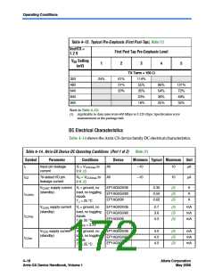
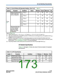
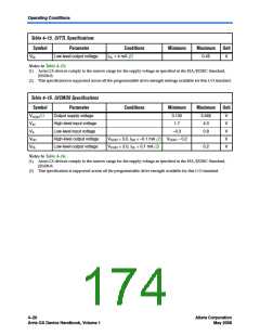
Operating Conditions
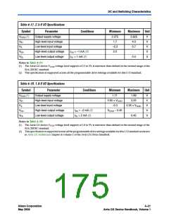
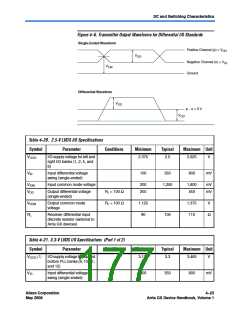
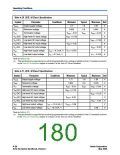
Table 4–19. 1.5-V I/O Specifications
Symbol
VCCIO (1)
VIH
Parameter
Output supply voltage
High-level input voltage
Low-level input voltage
High-level output voltage
Low-level output voltage
Conditions
Minimum
1.425
Maximum
1.575
Unit
V
0.65 VCCIO
–0.3
VCCIO + 0.3
0.35 VCCIO
V
VIL
V
VOH
IOH = –2 mA (2)
IOL = 2 mA (2)
0.75 VCCIO
V
VOL
0.25 VCCIO
V
Notes to Table 4–19:
(1) The Arria GX device VCCIO voltage level support of 1.5 to 5% is narrower than defined in the normal range of the
EIA/JEDEC standard.
(2) This specification is supported across all the programmable drive settings available for this I/O standard as shown
in Arria GX Architecture chapter in volume 1 of the Arria GX Device Handbook.
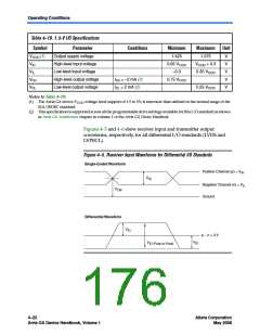
Figures 4–5 and 4–6 show receiver input and transmitter output
waveforms, respectively, for all differential I/O standards (LVDS and
LVPECL).
Figure 4–5. Receiver Input Waveforms for Differential I/O Standards
Single-Ended Waveform
Positive Channel (p) = V
IH
V
ID
Negative Channel (n) = V
IL
V
CM
Ground
Differential Waveform
V
ID
p − n = 0 V
V
V
ID
ID (Peak-to-Peak)
4–22
Arria GX Device Handbook, Volume 1
Altera Corporation
May 2008

 ALTERA [ ALTERA CORPORATION ]