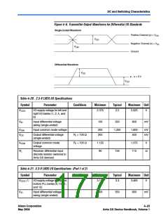
DC and Switching Characteristics
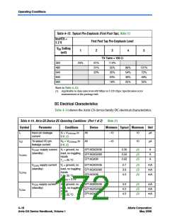
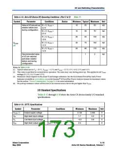
Table 4–14. Arria GX Device DC Operating Conditions (Part 2 of 2)
Note (1)
Symbol
Parameter
Conditions
Device
Minimum Typical Maximum Unit
Value of I/O pin pull-up Vi = 0, VCCIO
=
=
=
=
=
10
15
30
40
50
25
35
50
75
90
1
50
kΩ
kΩ
kΩ
kΩ
kΩ
kΩ
resistor before and
during configuration
3.3 V
Vi = 0, VCCIO
2.5 V
70
Vi = 0, VCCIO
1.8 V
100
150
170
2
Vi = 0, VCCIO
1.5 V
RCONF
(4)
Vi = 0, VCCIO
1.2 V
Recommended value
of I/O pin external
pull-down resistor
before and during
configuration
Notes to Table 4–14:
(1) Typical values are for TA = 25 °C, VCCINT = 1.2 V, and VCCIO = 1.2 V, 1.5 V, 1.8 V, 2.5 V, and 3.3 V.
(2) This value is specified for normal device operation. The value may vary during power-up. This applies for all VCCIO
settings (3.3, 2.5, 1.8, 1.5, and 1.2 V).
(3) Maximum values depend on the actual TJ and design utilization. See the Excel-based PowerPlay Early Power
Estimator (available at www.altera.com) or the Quartus® II PowerPlay Power Analyzer feature for maximum values.
See the section “Power Consumption” on page 4–34 for more information.
(4) Pin pull-up resistance values will be lower if an external source drives the pin higher than VCCIO
.
I/O Standard Specifications
Tables 4–15 through 4–38 show the Arria GX device family I/O standard
specifications.
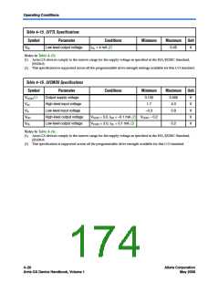
Table 4–15. LVTTL Specifications
Symbol
VCCIO (1)
VIH
Parameter
Conditions
Minimum
3.135
1.7
Maximum
3.465
4.0
Unit
V
Output supply voltage
High-level input voltage
Low-level input voltage
High-level output voltage
V
VIL
–0.3
0.8
V
VOH
IOH = –4 mA (2)
2.4
V
Altera Corporation
May 2008
4–19
Arria GX Device Handbook, Volume 1

 ALTERA [ ALTERA CORPORATION ]