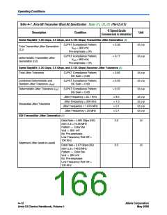
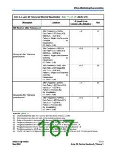
Operating Conditions
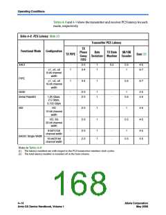
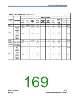
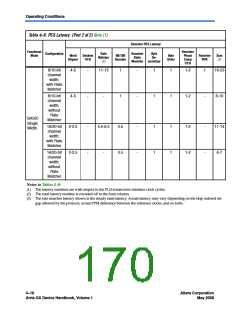
Table 4–9. PCS Latency (Part 2 of 2) Note (1)
Receiver PCS Latency
Functional
Mode
Receiver
Phase
Comp
Configuration
Rate
Matcher
(3)
Receiver
State
Byte
De-
Word
Aligner
Deskew
FIFO
8B/10B
Decoder
Byte
Order
Receiver
PIPE
Sum
(2)
Machine serializer
FIFO
8/10-bit
channel
width;
4-5
-
11-13
1
-
1
1
1-2
1
19-23
with Rate
Matcher
8/10-bit
channel
width;
4-5
-
-
1
-
1
1
1-2
-
8-10
without
Rate
Matcher
BASIC
Single
Width
16/20-bit
channel
width;
2-2.5
2-2.5
-
-
5.5-6.5
0.5
0.5
-
-
1
1
1
1
1-2
1-2
-
-
11-14
6-7
with Rate
Matcher
16/20-bit
channel
width;
-
without
Rate
Matcher
Notes to Tables 4–9:
(1) The latency numbers are with respect to the PLD-transceiver interface clock cycles.
(2) The total latency number is rounded off in the Sum column.
(3) The rate matcher latency shown is the steady state latency. Actual latency may vary depending on the skip ordered set
gap allowed by the protocol, actual PPM difference between the reference clocks, and so forth.
4–16
Altera Corporation
May 2008
Arria GX Device Handbook, Volume 1

 ALTERA [ ALTERA CORPORATION ]