7–14
Chapter 7: High-Speed Differential Interfaces in the Cyclone III Device Family
High-Speed I/O Standards Support
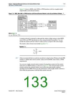
Figure 7–11 shows the differential SSTL Class II interface.
Figure 7–11. Differential SSTL Class II Interface
VTT
VTT
VTT
VTT
Output Buffer (1)
Receiver
Note to Figure 7–11:
(1) PLL output clock pins do not support differential SSTL-18 Class II I/O standard.
Differential HSTL I/O Standard Support in the Cyclone III Device Family
The differential HSTL I/O standard is used for the applications designed to operate in
0 V to 1.2 V, 0 V to 1.5 V, or 0 V to 1.8 V HSTL logic switching range. The Cyclone III
device family supports differential HSTL-18, HSTL-15, and HSTL-12 I/O standards.
The differential HSTL input standard is available on GCLK pins only, treating the
differential inputs as two single-ended HSTL and only decoding one of them. The
differential HSTL output standard is only supported at the PLL#_CLKOUTpins using
two single-ended HSTL output buffers (PLL#_CLKOUTp and PLL#_CLKOUTn), with the
second output programmed to have opposite polarity.
The differential HSTL I/O standard requires two differential inputs with an external
reference voltage (VREF), as well as an external termination voltage (VTT) of 0.5 × VCCIO
to which termination resistors are connected.
f
For more information about the differential HSTL signaling characteristics, refer to the
I/O Features in the Cyclone III Device Family, Cyclone III Device Data Sheet, and Cyclone III
LS Device Data Sheet chapters.
Figure 7–12 shows the differential HSTL Class I interface.
Figure 7–12. Differential HSTL Class I Interface
VTT
VTT
50 Ω
50 Ω
Output Buffer
Receiver
Z
= 50 Ω
= 50 Ω
0
Z
0
Cyclone III Device Handbook
Volume 1
December 2011 Altera Corporation

 ALTERA [ ALTERA CORPORATION ]