Chapter 7: High-Speed Differential Interfaces in the Cyclone III Device Family
7–9
High-Speed I/O Standards Support
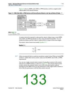
Figure 7–4 shows a typical BLVDS topology with multiple transmitter and receiver
pairs.
Figure 7–4. BLVDS Topology with Cyclone III Device Family Transmitters and Receivers
V
V
CC
CC
100 kΩ
100 kΩ
50 Ω
50 Ω
50 Ω
50 Ω
50 Ω
50 Ω
50 Ω
R
T
R
T
50
Ω
100 kΩ
GND
100 k Ω
GND
Output
Data
Output
Data
Output
Data
Input
Data
Input
Data
Input
Data
The BLVDS I/O standard is supported on all I/O banks of the Cyclone III device
family. The BLVDS transmitter uses two single-ended output buffers with the second
output buffer programmed as inverted, while the BLVDS receiver uses a true LVDS
input buffer. The transmitter and receiver share the same pins. An output-enabled (OE
signal is required to tristate the output buffers when the LVDS input buffer receives a
signal.
)
f
f
For more information about BLVDS I/O features and electrical specifications, refer to
the I/O Features in the Cyclone III Device Family chapter in volume 1 of the Cyclone III
Device Handbook and the Cyclone III Device Data Sheet and Cyclone III LS Device Data
Sheet chapters.
For more information and design examples about implementing the BLVDS interfaces
in the Cyclone III device family, refer to AN 522: Implementing Bus LVDS Interface in
Supported Altera Device Families.
Designing with BLVDS
The BLVDS bidirectional communication requires termination at both ends of the bus
in BLVDS. The termination resistor (RT) must match the bus differential impedance,
which in turn depends on the loading on the bus. Increasing the load decreases the
bus differential impedance. With termination at both ends of the bus, termination is
not required between the two signals at the input buffer. A single series resistor (RS) is
required at the output buffer to match the output buffer impedance to the
transmission line impedance. However, this series resistor affects the voltage swing at
the input buffer. The maximum data rate achievable depends on many factors.
1
Altera recommends that you perform simulation using the IBIS model while
considering factors such as bus loading, termination values, and output and input
buffer location on the bus to ensure that the required performance is achieved.
December 2011 Altera Corporation
Cyclone III Device Handbook
Volume 1

 ALTERA [ ALTERA CORPORATION ]