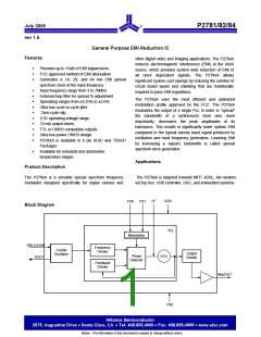
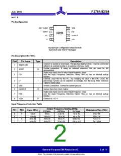
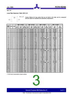
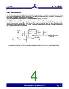
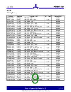
July 2005
P2781/82/84
rev 1.5
Absolute Maximum Ratings
Symbol
VDD
VI
Parameter
Rating
(VSS – 0.5) to 7
(VSS-0.5) to (VDD+0.5)
(VSS-0.5) to (VDD + 0.5)
-50 to +50
Unit
V
Supply voltage, DC
Input voltage, DC
V
VO
Output voltage, DC
V
IIK
Input clamp current (VI<0 or VI>VDD)
Output clamp current (VI<0 or VI>VDD)
Storage temperature
mA
mA
°C
°C
°C
°C
IOK
-50 to +50
TS
-65 to +125
TA
Ambient temperature range, under bias
Junction temperature
-55 to 125
TJ
150
Lead temperature (soldering 10 sec)
260
Input static discharge voltage protection
(As per JEDEC STD22- A114-B)
2
kV
Note: These are stress ratings only and functional operation is not implied. Exposure to absolute maximum ratings for extended periods may affect device
reliability.
DC Electrical Characteristics
(Test condition: All parameters are measured at room temperature (+25°C) unless otherwise stated)
Symbol
VIL
Parameter
Min
VSS – 0.3
2.0
Typ
Max
0.8
Unit
V
Input low voltage
-
-
VIH
Input high voltage
Input low current
VDD +0.3
V
IIL
-
-
60
60
-
-
µA
µA
(internal input pull-up resistor on FS0 and FS1)
Input high current
IIH
(internal input pull-up resistor on FS0 and FS1)
IXOL
IXOH
XOUT output low current
XOUT output high current
-
-
10
10
-
-
mA
mA
VOL
VOH
Output low voltage (VDD = 3.3V, IOL = 20mA)
-
-
-
0.4
V
Output high voltage (VDD = 3.3V, IOH = 20mA)
Static supply current
2.5
-
-
V
IDD
-
3
-
mA
Typical dynamic supply current
(25pF scope probe loading)
ICC
5.2 at 3MHz
3.0
21.2 at 82MHz mA
3.6
VDD
Operating voltage
3.3
V
General Purpose EMI Reduction IC
5 of 11
Notice: The information in this document is subject to change without notice.

 ALSC [ ALLIANCE SEMICONDUCTOR CORPORATION ]