AS7C252MPFD18A
®
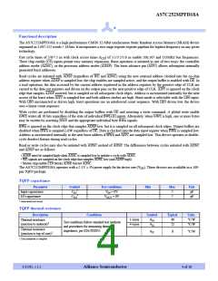
Absolute maximum ratings
Parameter
Power supply voltage relative to GND
Input voltage relative to GND (input pins)
Input voltage relative to GND (I/O pins)
Power dissipation
Symbol
Min
–0.3
–0.3
–0.3
–
Max
+3.6
Unit
V
VDD, VDDQ
VIN
VDD + 0.3
VDDQ + 0.3
1.8
V
VIN
V
Pd
W
Short circuit output current
IOUT
Tstg
–
20
mA
oC
oC
Storage temperature
–65
–65
+150
Temperature under bias
Tbias
+135
Stresses greater than those listed under “Absolute maximum ratings” may cause permanent damage to the device. This is a stress rating only, and functional operation of the
device at these or any other conditions outside those indicated in the operational sections of this specification is not implied. Exposure to absolute maximum rating conditions
may affect reliability.
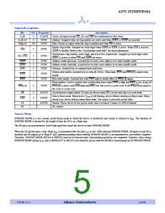
Recommended operating conditions
Parameter
Supply voltage for inputs
Supply voltage for I/O
Ground supply
Symbol
VDD
Min
2.375
2.375
0
Nominal
Max
2.625
2.625
0
Unit
V
2.5
2.5
0
VDDQ
Vss
V
V
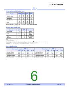
DC electrical characteristics
Parameter
Input leakage current†
Output leakage current
Sym
|ILI|
Conditions
VDD = Max, OV < VIN < VDD
Min
-2
Max
Unit
2
2
µA
µA
V
|ILO
|
OE ≥ VIH, VDD = Max, OV < VOUT < VDDQ
Address and control pins
I/O pins
-2
1.7*
1.7*
-0.3**
-0.3**
1.7
VDD+0.3
Input high (logic 1) voltage
Input low (logic 0) voltage
VIH
VDDQ+0.3
V
Address and control pins
I/O pins
0.7
0.7
–
V
VIL
V
Output high voltage
Output low voltage
VOH
VOL
IOH = –4 mA, VDDQ = 2.375V
IOL = 8 mA, VDDQ = 2.625V
V
–
0.7
V
† LBO and ZZ pins have an internal pull-up or pull-down, and input leakage = ±10 µA.
*
V
max < VDD +1.5V for pulse width less than 0.2 X t
CYC
IH
**
V
min = -1.5 for pulse width less than 0.2 X t
CYC
IL
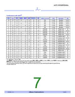
IDD operating conditions and maximum limits
Parameter
Sym
Conditions
-200
450
-166
-133
Unit
CE0 < VIL, CE1 > VIH, CE2 < VIL, f = fMax
,
Operating power supply current1
ICC
400
150
350
mA
IOUT = 0 mA, ZZ < VIL
All VIN ≤ 0.2V or >
V
– 0.2V, Deselected,
DD
ISB
170
140
f = fMax, ZZ < VIL
Deselected, f = 0, ZZ < 0.2V,
all VIN ≤ 0.2V or ≥ VDD – 0.2V
Standby power supply current
mA
ISB1
ISB2
90
80
90
80
90
80
Deselected, f = f , ZZ
≥
V
– 0.2V,
Max
DD
all VIN ≤ VIL or ≥ VIH
1 I given with no output loading. I increases with faster cycle times and greater output loading.
CC
CC
2/11/05, v.1.1
Alliance Semiconductor
8 of 18

 ALSC [ ALLIANCE SEMICONDUCTOR CORPORATION ]