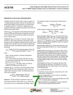
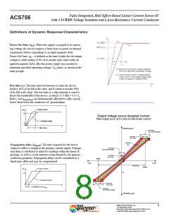
Fully Integrated, Hall Effect-Based Linear Current Sensor IC
with 3 kVRMS Voltage Isolation and a Low-Resistance Current Conductor
ACS756
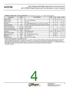
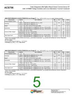
COMMON OPERATING CHARACTERISTICS1 over full range of TOP, and VCC = 5 V, unless otherwise specified
Characteristic
Symbol
Test Conditions
Min.
Typ.
5.0
10
Max.
5.5
14
–
Units
V
Supply Voltage2
VCC
3
Supply Current
ICC
VCC = 5.0 V, output open
–
mA
μs
Power On Time
tPO
TA = 25°C
–
35
Rise Time
tr
IP = three-quarter scale of IP+, TA = 25°C, COUT = 0.47 nF
–
3
–
μs
Internal Bandwidth3
Output Load Resistance
Output Load Capacitance
Primary Conductor Resistance
Symmetry
BWi
–3 dB; IP is 10 A peak-to-peak; 100 pF from VIOUT to GND
–
120
–
–
kHz
kΩ
nF
RLOAD(MIN)
CLOAD(MAX)
RPRIMARY
ESYM
VIOUT to GND
VIOUT to GND
TA = 25°C
4.7
–
–
–
10
–
–
130
100
μꢀ
%
Over half-scale of Ip
98.5
101.5
Bidirectional 0 A Output
Magnetic Offset Error
Ratiometry
VOUT(QBI)
IERROM
VRAT
IP = 0 A, TA = 25°C
–
–
–
–
VCC/2
±0.23
100
1
–
–
–
–
V
A
IP = 0 A, after excursion of 100 A
VCC = 4.5 to 5.5 V
%
μs
Propagation Time
tPROP
TA = 25°C, COUT = 100 pF,
1Device is factory-trimmed at 5 V, for optimal accuracy.
2Devices are programmed for maximum accuracy at 5.0 V VCC levels. The device contains ratiometry circuits that accurately alter the 0 A Output Volt-
age and Sensitivity level of the device in proportion to the applied VCC level. However, as a result of minor nonlinearities in the ratiometry circuit ad-
ditional output error will result when VCC varies from the 5 V VCC level. Customers that plan to operate the device from a 3.3 V regulated supply should
contact their local Allegro sales representative regarding expected device accuracy levels under these bias conditions.
3Guaranteed by design.
Allegro MicroSystems, Inc.
115 Northeast Cutoff
4
Worcester, Massachusetts 01615-0036 U.S.A.
1.508.853.5000; www.allegromicro.com

 ALLEGRO [ ALLEGRO MICROSYSTEMS ]