6B595
8-BIT SERIAL-INPUT,
DMOS POWER DRIVER
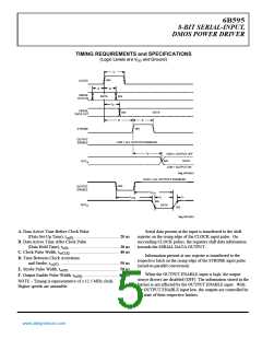
TIMING REQUIREMENTS and SPECIFICATIONS
(Logic Levels are VDD and Ground)
C
50%
CLOCK
A
B
SERIAL
DATA IN
DATA
50%
t
p
SERIAL
DATA OUT
50%
DATA
D
E
50%
STROBE
OUTPUT
ENABLE
LOW = ALL OUTPUTS ENABLED
t
p
HIGH = OUTPUT OFF
50%
DATA
LOW = OUTPUT ON
Dwg. WP-029-2
OUT
N
HIGH = ALL OUTPUTS DISABLED
50%
OUTPUT
ENABLE
t
PLH
t
t
t
r
PHL
f
90%
OUT
N
DATA
10%
Dwg. WP-030-2
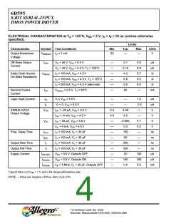
A. Data Active Time Before Clock Pulse
(Data Set-Up Time), tsu(D) .......................................... 20 ns
B. Data Active Time After Clock Pulse
(Data Hold Time), th(D) .............................................. 20 ns
C. Clock Pulse Width, tw(CLK) ............................................. 40 ns
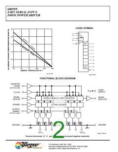
Serial data present at the input is transferred to the shift
register on the rising edge of the CLOCK input pulse. On
succeeding CLOCK pulses, the registers shift data information
towards the SERIAL DATA OUTPUT.
Information present at any register is transferred to the
respective latch on the rising edge of the STROBE input pulse
(serial-to-parallel conversion).
D. Time Between Clock Activation
and Strobe, tsu(ST) ....................................................... 50 ns
E. Strobe Pulse Width, tw(ST) .............................................. 50 ns
F. Output Enable Pulse Width, tw(OE) ................................ 4.5 µs
NOTE – Timing is representative of a 12.5 MHz clock.
Higher speeds are attainable.
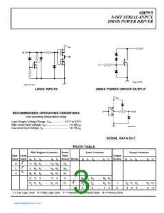
When the OUTPUT ENABLE input is high, the output
source drivers are disabled (OFF). The information stored in the
latches is not affected by the OUTPUT ENABLE input. With
the OUTPUT ENABLE input low, the outputs are controlled by
the state of their respective latches.
www.allegromicro.com

 ALLEGRO [ ALLEGRO MICROSYSTEMS ]