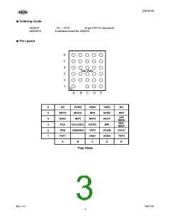
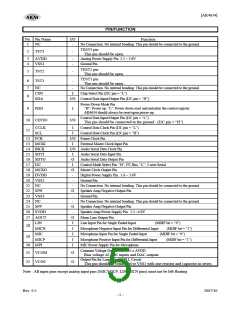
[AK4634]
PIN/FUNCTION
No. Pin Name
I/O
-
Function
1
NC
No Connection. No internal bonding. This pin should be connected to the ground.
TEST3 pin
This pin should be open.
Analog Power Supply Pin 2.2 ~ 3.6V
2
TST3
-
3
4
AVDD
VSS1
-
-
Ground Pin.
TEST2 pin
This pin should be open.
TEST1 pin
This pin should be open.
5
TST2
TST1
-
-
6
7
NC
-
I
No Connection. No internal bonding. This pin should be connected to the ground.
CSN
SDA
Chip Select Pin (I2C pin = “L”)
8
I/O Control Data Input/Output Pin (I2C pin = “H”)
Power-Down Mode Pin
“H”: Power up, “L”: Power down reset and initialize the control register.
AK4634 should always be reset upon power-up.
9
PDN
I
Control Data Input/Output Pin (I2C pin = “L”)
This pin should be connected to the ground. (I2C pin = “H”)
10 CDTIO
I/O
CCLK
I
I
Control Data Clock Pin (I2C pin = “L”)
Control Data Clock Pin (I2C pin = “H”)
11
SCL
12 FCK
13 MCKI
14 BICK
15 SDTI
16 SDTO
17 I2C
I/O Frame Clock Pin
I
External Master Clock Input Pin
I/O Audio Serial Data Clock Pin
I
O
I
Audio Serial Data Input Pin
Audio Serial Data Output Pin
Control Mode Select Pin “H”: I2C Bus, “L”: 3-wire Serial
18 MCKO
19 DVDD
20 VSS2
21 NC
O
-
Master Clock Output Pin
Digital Power Supply Pin 1.6 ~ 3.6V
Ground Pin.
-
-
No Connection. No internal bonding. This pin should be connected to the ground.
Speaker Amp Negative Output Pin
22 SPN
23 VSS3
24 NC
O
-
Ground Pin.
-
No Connection. No internal bonding. This pin should be connected to the ground.
Speaker Amp Negative Output Pin
25 SPP
O
-
26 SVDD
27 AOUT
Speaker Amp Power Supply Pin 2.2 ~4.0V
Mono Line Output Pin
O
I
LIN
28
Line Input Pin for Single Ended Input
(MDIF bit = “0”)
(MDIF bit = “1”)
(MDIF bit = “0”)
(MDIF bit = “1”)
MICN
I
Microphone Negative Input Pin for Differential Input
Microphone Input Pin for Single Ended Input
Microphone Positive Input Pin for Differential Input
MIC Power Supply Pin for Microphone
MIC
29
I
MICP
I
30 MPI
I
Common Voltage Output Pin, 0.45 x AVDD
Bias voltage of ADC inputs and DAC outputs.
Output Pin for Loop Filter of PLL Circuit
31 VCOM
O
O
32 VCOC
This pin should be connected to VSS1 with one resistor and capacitor in series.
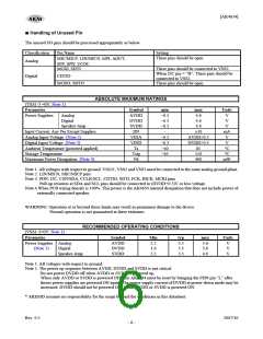
Note : All input pins except analog input pins (MIC/MICP, LIN/MICN pins) must not be left floating
Rev. 0.5
2007/10
- 5 -

 AKM [ ASAHI KASEI MICROSYSTEMS ]