[AK4634]
(default)
R and C of
VCOC pin
PLL Lock
Time
(max)
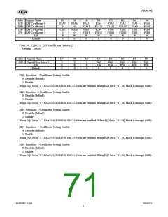
PLL3 PLL2 PLL1 PLL0 PLL Reference
Input
Frequency
Mode
bit
bit
bit
bit
Clock Input Pin
C[F]
R[Ω]
6.8k
10k
10k
10k
10k
10k
10k
10k
0
1
2
3
6
0
0
0
0
0
0
1
1
0
0
0
0
1
1
1
0
0
1
1
1
1
0
0
0
1
0
1
0
1
0
1
FCK pin
BICK pin
BICK pin
BICK pin
MCKI pin
MCKI pin
MCKI pin
MCKI pin
N/A
1fs
16fs
32fs
220n
4.7n
4.7n
4.7n
4.7n
4.7n
10n
160ms
2ms
2ms
64fs
2ms
12MHz
24MHz
13.5MHz
27MHz
20ms
20ms
20ms
20ms
7
12
13
Others
1
10n
Others
Note 29. the tolerance of R is ±5%, the tolerance of C is ±30%
Table 4. Setting of PLL Mode (*fs: Sampling Frequency, N/A: Not available)
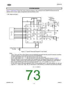
1. Grounding and Power Supply Decoupling
The AK4634 requires careful attention to power supply and grounding arrangements. AVDD, DVDD and SVDD are
usually supplied from the system’s analog supply. If AVDD, DVDD and SVDD are supplied separately, the correct
power up sequence should be observeVSS21, VSS2 and VSS3 of the AK4634 should be connected to the analog ground
plane. System analog ground and digital ground should be connected together near to where the supplies are brought onto
the printed circuit board. Decoupling capacitors should be as near to the AK4634 as possible, with the small value
ceramic capacitor being the nearest.
2. Voltage Reference
VCOM is a signal ground of this chip. A 2.2μF electrolytic capacitor in parallel with a 0.1μF ceramic capacitor attached
to the VCOM pin eliminates the effects of high frequency noise. No load current may be drawn from the VCOM pin. All
signals, especially clocks, should be kept away from the VCOM pin in order to avoid unwanted coupling into the
AK4634.
3. Analog Inputs
The Mic and Line inputs supports single-ended and differential. The input signal range scales with nominally at 0.06 x
AVDD Vpp@MIC-amp gain 20dB for the Mic input and 0.6 x AVDD Vpp@MIC-amp gain 20dB for the Beep input,
centered around the internal common voltage (approx. 0.45 x AVDD). Usually the input signal is AC coupled with a
capacitor. The cut-off frequency is fc = (1/2πRC). The AK4634 can accept input voltages from VSS1 to AVDD.
4. Analog Outputs
The input data format for the DAC is 2’s complement. The output voltage is a positive full scale for 7FFFH(@16bit) and
a negative full scale for 8000H(@16bit). The theoretical figure for 0000H (@16bit) is VCOM voltage. Mono Line Output
from the AOUT pin is centered at 0.45 x AVDD (typ).
MS0983-E-00
2008/07
- 75 -

 AKM [ ASAHI KASEI MICROSYSTEMS ]