ASAHI KASEI
[AK4571]
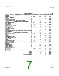
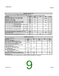
Digital DC Characteristics
Ta=0 - 70°C; VD=3.0 - 3.6V; DGND=0V Measurement under static state
All digital pins except DP, DN. Schmitt hysteresis level of RSTN pin and levels of all test pins will not be tested.
Parameter
Symbol
VIH
VIL
VIHR
VILR
VIHR
VILR
VOH
Min
70%VD
Typ
Max
30%VD
0.8
Units
EPDI,EPEN, EPSEL, pin “H” level input voltage
EPDI, EPEN, EPSEL pin “L” level input voltage
RSTN pin “H” level voltage
V
V
V
V
V
V
V
2.4
2.4
2.4
RSTN pin “L” level voltage
IMUTE, OMUTE, INC, DEC pin “H” level voltage
IMUTE, OMUTE, INC, DEC pin “L” level voltage
SUSN, EPSW, STBY, EMSW, MSTAT pin
0.8
“H” level output voltage IOH= 2mA
SUSN, EPSW, STBY, EMSW, MSTAT pin
“L” level output voltage
CS, SK, EPAO pin “H” level output voltage
VOL
VOH
VOL
0.6
0.6
V
V
V
IOL= -2mA
IOH= 2mA
IOL= -2mA
2.4
2.0
CS, SK, EPAO pin “L” level output voltage
DP, DN Single Ended Receiver Threshold for “H” level
DP, DN Single Ended Receiver Threshold for pin “L” level
Input Leakage Current
VIHR
VILR
Iin
V
V
µA
kΩ
0.8
±10
Rpd
100
Pull down Resistance (only EPDI pin)@3.3V Ta=25°C
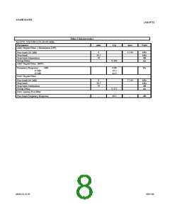
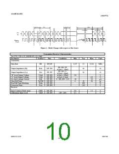
Switching Characteristics
Ta=25°C, VA=VD=3.3V
Parameter
Master Clock Frequency
Symbol
MCLK
Wrst
Min
-
1.0
Typ
12.000
Max
-
Units
MHz
us
Reset input width @RSTN pin(low active)
Time Width for USB Reset Signal Recognition
DP<VseL & DN< VseL to USB Reset mode
Device Ready Time from USB Reset
After releasing from USB Reset to Device Ready
(Transaction can start)
Time Width for Suspend Recognition
Idle state ( DP > VseL & DN < VseL )
to Suspend mode
µs
Trst_rec
3.0
Tdrr
10
ms
ms
ms
Tsus_rec
Tresm
4.36
Resume Time from Suspend
First flip of DP/DN from Idle state
To Device Ready*)
30
Imute input width with @IMUTE pin(High active)
Omute,Dec,Inc input width with @OMUTE,DEC,INC
pin (High active)
Wimute
Wodi
10.005
2.001
ms
ms
Device Ready: VREF, X’tal oscillator and PLL are stable and standard bus transactions can proceed
MS0153-E-03
2005/06
- 9 -

 AKM [ ASAHI KASEI MICROSYSTEMS ]