[AK4438]
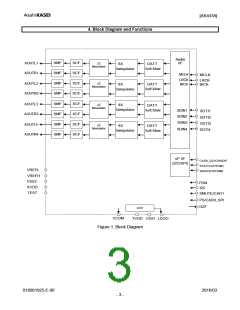
■ Pin Functions
No. Pin Name
I/O
Function
PD state
1
2
3
4
5
6
7
MCLK
BICK
I
I
I
I
I
I
I
O
Hi-z
Hi-z
Hi-z
Hi-z
Hi-z
External Master Clock Input Pin
Audio Serial Data Clock Pin
Input Channel Clock Pin
Audio Serial Data Input
Audio Serial Data Input
Audio Serial Data Input
Audio Serial Data Input
Zero Input Detect in I2C Bus or 3-wire serial control mode
LRCK
SDTI1
SDTI2
SDTI3
SDTI4
DZF
Hi-z
Hi-z
50kΩ
Pull-down
8
Power-Down & Reset Pin.
9
PDN
I
I
Hi-z
When “L”, the AK4438 is powered-down and the control registers are reset to
default state.
Soft Mute Pin in Parallel control mode.
SMUTE
When this pin is changed to “H”, soft mute cycle is initiated. When returning
10
Hi-z
“L”, the output mute releases.
CAD1
SDA
11 CDTI
TDM0
SCL
12 CCLK
TDM1
I
Chip Address 1 Pin in I2C Bus or 3-wire serial control mode
Control Data Input Pin in I2C Bus serial control mode
Control Data Input Pin in 3-wire serial control mode
TDM Mode select pin in Parallel control mode.
Control Data Clock Pin in I2C Bus serial control mode
Control Data Clock Pin in 3-wire serial control mode
TDM Mode select pin in Parallel control mode.
Chip Address 0 Pin in I2C Bus serial control mode
Chip Select Pin in 3-wire serial control mode
Audio Data Format Select in Parallel control mode.
“L”: 32bit MSB, “H”: 32bit I2S
I/O
I
I
I
I
I
I
I
Hi-z
Hi-z
CAD0_I2C
CSN
13
Hi-z
Hi-z
DIF
I
I
(I2C pin = “H”) Control Mode Select Pin
PS
“L”: I2C Bus serial control mode, “H”: Parallel control mode.
(I2C pin = “L”) Chip Address 0 Pin in 3-wire serial control mode
Lch Analog Output Pin
14
CAD0_SPI
AOUTL1
AOUTR1
AOUTL2
AOUTR2
I
O
O
O
O
-
Hi-z
Hi-z
Hi-z
Hi-z
Hi-z
Hi-z
15
16
17
18
Rch Analog Output Pin
Lch Analog Output Pin
Rch Analog Output Pin
Positive Voltage Reference Input Pin, AVDD
Negative Voltage Reference Input Pin, VSS2
Common Voltage Output Pin, AVDDx1/2
Large external capacitor around 2.2µF is used to reduce power-supply noise.
Analog Ground Pin
Analog Power Supply Pin, 3.0V3.6V
Lch Analog Output Pin
Rch Analog Output Pin
19 VREFH
20 VREFL
-
500Ω
Pull-down
-
21 VCOM
O
VSS2
AVDD
AOUTL3
AOUTR3
AOUTL4
AOUTR4
-
-
O
O
O
O
22
23
24
25
26
27
-
Hi-z
Hi-z
Hi-z
Hi-z
Lch Analog Output Pin
Rch Analog Output Pin
25kΩ
Pull-down
This pin must be connected to VSS1.
28 TEST
-
Control Mode Select Pin
29 I2C
I
Hi-z
“L”: 3-wire serial control mode
“H”: I2C Bus serial control mode or Parallel control mode.
Digital Power Supply Pin, 1.7V3.6V
Digital Ground Pin
30 TVDD
-
-
-
-
VSS1
31
O
580Ω
Pull-down
LDO Output Pin.
This pin must be connected to ground with 2.2uF ±50%.
32 LDOO
Note 1. All digital input pins must not be allowed to float.
016001925-E-00
2016/03
- 5 -

 AKM [ ASAHI KASEI MICROSYSTEMS ]