ASAHI KASEI
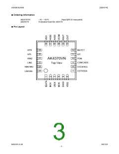
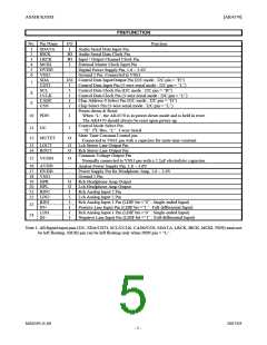
No. Pin Name
[AK4370]
PIN/FUNCTION
I/O
I
Function
1
2
3
4
5
6
SDATA
BICK
LRCK
MCKI
DVDD
VSS2
SDA
Audio Serial Data Input Pin
I/O Audio Serial Data Clock Pin
I/O Input / Output Channel Clock Pin
I
-
-
External Master Clock Input Pin
Digital Power Supply Pin, 1.6 ∼ 3.6V
Ground 2 Pin. Connected to VSS1.
I/O Control Data Input/Output Pin (I2C mode : I2C pin = “H”)
7
8
9
CDTI
SCL
I
I
I
I
I
Control Data Input Pin (3-wire serial mode : I2C pin = “L”)
Control Data Clock Pin (I2C mode : I2C pin = “H”)
Control Data Clock Pin (3-wire serial mode : I2C pin = “L”)
Chip Address 0 Select Pin (I2C mode : I2C pin = “H”)
Chip Select Pin (3-wire serial mode : I2C pin = “L”)
Power-down & Reset
CCLK
CAD0
CSN
10 PDN
I
When “L”, the AK4370 is in power-down mode and is held in reset.
The AK4370 should always be reset upon power-up.
Control Mode Select Pin
11 I2C
I
“H”: I2C Bus, “L”: 3-wire Serial
Mute Time Constant Control pin
Connected to VSS1 pin with a capacitor for mute time constant.
12 MUTET
O
13 LOUT
14 ROUT
O
O
Lch Stereo Line Output Pin
Rch Stereo Line Output Pin
Common Voltage Output Pin
Normally connected to VSS1 pin with a 2.2μF electrolytic capacitor.
Analog Power Supply Pin, 1.6 ∼ 3.6V
Power Supply Pin for Headphone Amp, 1.6 ∼ 3.6V
Ground 1 Pin
Rch Headphone Amp Output
Lch Headphone Amp Output
Rch Analog Input 2 Pin
Lch Analog Input 2 Pin
15 VCOM
O
16 AVDD
17 HVDD
18 VSS1
19 HPR
20 HPL
-
-
-
O
O
I
21 RIN2
22 LIN2
I
RIN1
IN+
LIN1
IN−
I
I
I
I
Rch Analog Input 1 Pin (LDIF bit =“0” : Single-ended Input)
Positive Line Input Pin (LDIF bit =“1” : Full-differential Input)
Rch Analog Input 1 Pin (LDIF bit =“0” : Single-ended Input)
Negative Line Input Pin (LDIF bit =“1” : Full-differential Input)
23
24
Note 1. All digital input pins (I2C, SDA/CDTI, SCL/CCLK, CAD0/CSN, SDATA, LRCK, BICK, MCKI, PDN) must not
be left floating. MCKI pin can be left floating only when PDN pin = “L”.
MS0595-E-00
2007/03
- 5 -

 AKM [ ASAHI KASEI MICROSYSTEMS ]