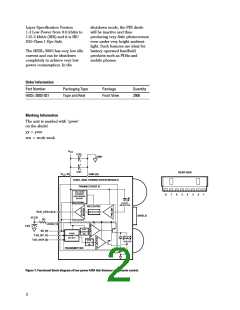
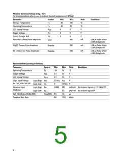
I/O Pins Configuration Table
Pin Symbol I/O Description
Notes
1
LEDA
I
IR and Remote
Control LED Driver
Tied through external resistor, R1, to VLED from 2.4 to 4.5 Volt
2
3
N.C.
–
I
No Connection
No Connection
TxD_IrDA
IrDA Transmitter Data
Input. Active High
Logic high turns on the IrDA LED. If held HIGH longer than
~50 µs, the IrDA LED is turned off. TxD_IrDA must be driven either
HIGH or LOW. Do not leave the pin floating
4
5
RxD_IrDA
SD
O
I
IrDA Receiver Data
Output. Active Low
Output is at LOW pulse response when light pulse is seen
Shutdown. Active High Complete shutdown TxD_IrDA, RxD_IrDA, and PIN diode. Do not
leave the pin floating
6
7
V
I
I
Supply Voltage
Regulated, 2.4 to 3.6 Volt
CC
TxD_RC
Remote Control
Transmission Input.
Active High
Logic high turns on the RC LED. If held HIGH longer than ~50 µs,
the RC LED is turned off. TxD_RC must be driven either HIGH or
LOW. Do not leave the pin floating
8
GND
I
Connect to System
Ground
Tie this pin to system ground
–
Shield
–
EMI Shield
Tie to system ground via a low inductance trace. For best
performance, do not tie it to the HSDL-3003 GND pin directly
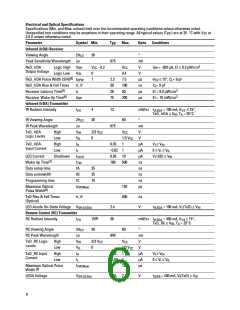
Recommended Application Circuit Components
Component
R1
Recommended Value
1.8 Ω ± 5%, 0.25 Watt for 2.4 ≤ VLED ≤ 2.7 V
2.7 Ω ± 5%, 0.25 Watt for 2.7 ≤ VLED ≤ 3.3 V
3.3 Ω ± 5%, 0.25 Watt for 3.0 ≤ VLED ≤ 3.6 V
4.7 Ω ± 5%, 0.25 Watt for 3.6 ≤ VLED ≤ 4.5 V
0.47 µF ± 20%, X7R Ceramic
[1]
CX1
[2]
CX2
6.8 µF ± 20%, Tantalum
CX3
6.8 µF ± 20%, Tantalum
Notes:
1. CX1 must be placed within 0.7 cm of HSDL-3003 to obtain optimum noise immunity.
2. The supply rejection performance can be enhanced by including CX2, as shown in Figure 1, in
environment with noisy power supplies.
3

 AGILENT [ AGILENT TECHNOLOGIES, LTD. ]