ADSemiconductor®
ANMG04 (4-CH Auto Sensitivity Calibration Capacitive Touch Sensor)
11 Recommended Circuit Diagram
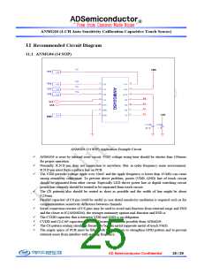
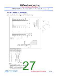
11.1 ANMG04 (14 SOP)
ANMG04 (14 SOP) Application Example Circuit
ANMG04 is reset by internal reset circuit. VDD voltage rising time should be shorter than 100msec
for proper operation.
Normally, R.N.D pin dose not connection to anywhere. But, in radio frequency noise environment,
R.N.D pin must form a pattern line on PCB.
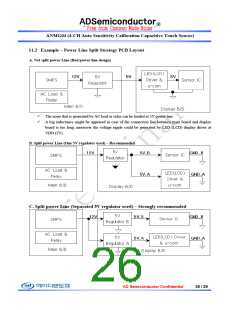
The VDD periodic voltage ripple over 50mV and the ripple frequency is lower than 10 kHz can cause
wrong sensitivity calibration. To prevent above problem, power (VDD, GND) line of touch circuit
should be separated from other circuit. Especially LED driver power line or digital switching circuit
power line certainly should be treated to be separated from touch circuit.
The CS patterns also should be routed as short as possible and the width of line might be about
0.25mm.
Parallel capacitor of CS pin could be useful in case detail sensitivity mediation is required such as for
complementation sensitivity difference between channels.
Serial connection resistor of CS pins may be used to avoid mal-function from external surge and ESD
and the closer to IC(ANMG04), the stronger immunity against mal-function and ESD is.
The CVDD capacitor that is between VDD and GND is an obligation.
CVDD and CLCAP capacitors should be located as close as possible from ANMG04.
The CS pattern routing should be formed by bottom metal (opposite metal of touch PAD).
The empty space of PCB must be filled with GND pattern to strengthen GND pattern and to prevent
external noise from interfere with sensing frequency.
AD Semiconductor Confidential
25 / 29

 ADI [ ADI ]