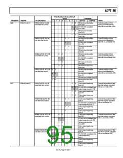
ADV7180
Bit (Shading Indicates
Default State)
User Sub Map
Address Register
Bit Description
7
6
5
4
3
2
1
0
Comments
Notes
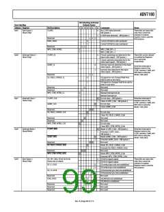
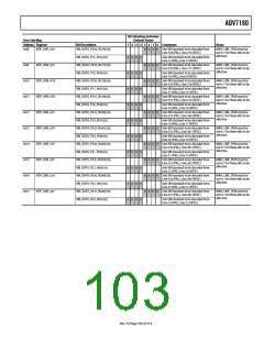
0x45
Raw Status 2
(Read Only)
CCAPD.
0
No CCAPD data detected—
VBI System 2
These bits are status bits
only; they cannot be
cleared or masked;
Register 0x46 is used for
this purpose
1
CCAPD data detected—VBI System 2
Reserved.
x
x
x
EVEN_FIELD.
0
1
Current SD field is odd numbered
Current SD field is even numbered
Reserved.
x
x
MPU_STIM_INTRQ.
0
1
MPU_STIM_INT = 0
MPU_STIM_INT = 1
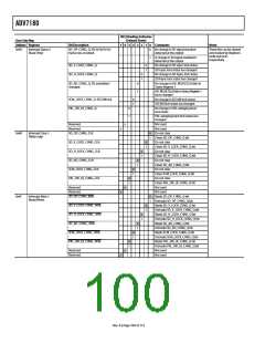
0x46
Interrupt Status 2
(Read Only)
CCAPD_Q.
GEMD_Q.
0
1
Closed captioning not detected in the
input video signal—VBI System 2
These bits can be cleared
or masked by Registers
0x47 and 0x48,
Closed captioning data detected in the
video input signal—VBI System 2
respectively
0
1
Gemstar data not detected in the input
video signal—VBI System 2
Note that interrupt in
Register 0x46 for the
CCAP, Gemstar, CGMS, and
WSS data is using the
Mode 1 data slicer
Gemstar data detected in the input
video signal—VBI System 2
Reserved.
x
x
SD_FIELD_CHNGD_Q.
0
1
SD signal has not changed field from
odd to even or vice versa
SD signal has changed Field from odd to
even or vice versa
Reserved.
x
Not used
Reserved.
x
Not used
MPU_STIM_INTRQ_Q.
0
1
Manual interrupt not set
Manual interrupt set
Do not clear—VBI System 2
Clears CCAPD_Q bit – VBI System 2
Do not clear
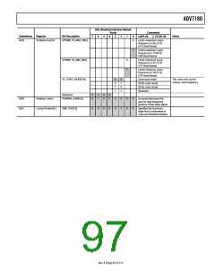
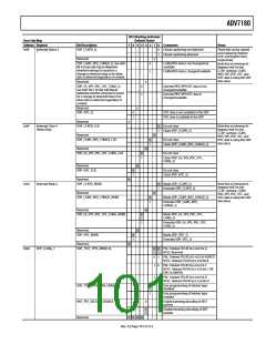
0x47
Interrupt Clear 2
(Write Only)
CCAPD_CLR.
GEMD_CLR.
0
1
Note that interrupt in
Register 0x46 for the
CCAP, Gemstar, CGMS, and
WSS data is using the
Mode 1 data slicer
0
1
Clears GEMD_Q bit
Reserved.
0 0
SD_FIELD_CHNGD_CLR.
0
1
Do not clear
Clears SD_FIELD_CHNGD_Q bit
Not used
Reserved.
x
Reserved.
x
Not used
MPU_STIM_INTRQ_CLR.
0
1
Do not clear
Clears MPU_STIM_INTRQ_Q bit
Masks CCAPD_Q bit—VBI System 2
0x48
Interrupt Mask 2
(Read/Write)
CCAPD_MSK
0
1
Note that interrupt in
Register 0x46 for the
CCAP, Gemstar, CGMS, and
WSS data is using the
Mode 1 data slicer.
.
Unmasks CCAPD_Q bit—
VBI System 2
GEMD_MSK
0
1
Masks GEMD_Q bit—VBI System 2
Unmasks GEMD_Q bit—VBI System 2
Not used
.
Reserved.
SD_FIELD_CHNGD_MSK
0 0
0
1
Masks SD_FIELD_CHNGD_Q bit
Unmasks SD_FIELD_CHNGD_Q bit
Not used
.
Reserved.
0
0
MPU_STIM_INTRQ_MSK
0
1
Masks MPU_STIM_INTRQ_Q bit
Unmasks MPU_STIM_INTRQ_Q bit
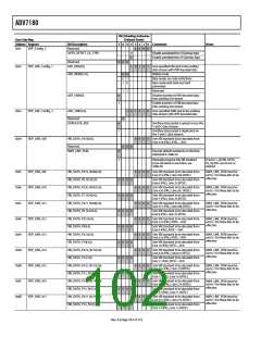
SD 60 Hz signal output
SD 50 Hz signal output
SD vertical sync lock not established
SD vertical sync lock established
SD horizontal sync lock not established
SD horizontal sync lock established
Not used
.
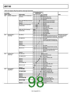
0x49
Raw Status 3
(Read Only)
SD_OP_50Hz. SD 60 Hz/50 Hz
frame rate at output.
0
1
These bits are status bits
only; they cannot be
cleared or masked;
Register 0x4A is used for
this purpose
SD_V_LOCK.
0
1
SD_H_LOCK.
0
1
Reserved.
x
SCM_LOCK.
0
1
SECAM lock not established
SECAM lock established
Not used
Reserved.
Reserved.
Reserved.
x
x
Not used
x
Not used
Rev. A | Page 99 of 112

 ADI [ ADI ]