ADV7170/ADV7171
TABLE OF CONTENTS
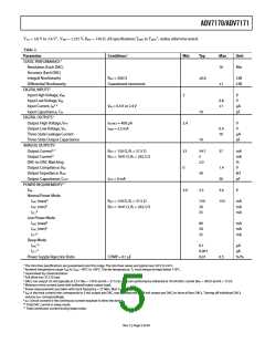
Specifications..................................................................................... 4
Mode Register 1 MR1 (MR17 to MR10)................................. 30
MR1 Bit Description.................................................................. 30
Mode Register 2 MR2 (MR27 to MR20)................................. 30
MR2 Bit Description.................................................................. 30
Mode Register 3 MR3 (MR37 to MR30).................................... 32
MR3 Bit Description.................................................................... 32
Mode Register 4 MR4 (MR47 to MR40)................................. 33
MR4 Bit Description.................................................................. 33
Dynamic Specifications ............................................................... 6
Timing Specifications .................................................................. 7
Timing Diagrams.......................................................................... 9
Absolute Maximum Ratings.......................................................... 10
Package Thermal Performance................................................. 10
ESD Caution................................................................................ 10
Pin Configuration and Function Descriptions........................... 11
General Description....................................................................... 13
Data Path Description................................................................ 13
Internal Filter Response............................................................. 14
Typical Performance Characteristics ........................................... 15
Features ............................................................................................ 18
Color Bar Generation ................................................................ 18
Square Pixel Mode...................................................................... 18
Color Signal Control.................................................................. 18
Burst Signal Control................................................................... 18
NTSC Pedestal Control ............................................................. 18
Pixel Timing Description .......................................................... 18
Subcarrier Reset.......................................................................... 18
Real-Time Control ..................................................................... 18
Video Timing Description ........................................................ 18
Power-On Reset.......................................................................... 26
SCH Phase Mode........................................................................ 26
MPU Port Description............................................................... 26
Register Accesses ........................................................................ 27
Register Programming................................................................... 28
Subaddress Register (SR7 to SR0) ............................................ 28
Register Select (SR5 to SR0)...................................................... 28
Mode Register 0 MR0 (MR07 to MR00)................................. 28
MR0 Bit Description.................................................................. 28
VSYNC
_3H (MR43).................................................................. 33
Timing Mode Register 0 (TR07 to TR00)............................... 33
TR0 Bit Description ................................................................... 34
Timing Mode Register 1 (TR17 to TR10)............................... 34
TR1 Bit Description ................................................................... 34
Subcarrier Frequency Registers 0 to 3 (FSC3 to FSC0)......... 35
Subcarrier Phase Registers (FP7 to FP0)................................. 35
Closed Captioning Even Field Data Register 1 to 0 (CED15 to
CED0) .......................................................................................... 35
Closed Captioning Odd Field Data Registers 1 to 0 (CCD15
to CCD0) ..................................................................................... 35
NTSC Pedestal/PAL Teletext Control Registers 3 to 0 (PCE15
to PCE0, PCO15 to PCO0)/(TXE15 to TXE0, TXO15 to
TXO0).......................................................................................... 36
Teletext Request Control Register TC07 (TC07 to TC00).... 36
CGMS_WSS Register 0 C/W0 (C/W07 to C/W00) .............. 36
C/W0 Bit Description................................................................ 36
CGMS_WSS Register 1 C/W1 (C/W17 to C/W10) .............. 37
C/W1 Bit Description................................................................ 37
CGMS Data Bits (C/W17 to C/W16)...................................... 37
CGMS_WSS Register 2 C/W1 (C/W27 to C/W20) .............. 37
C/W2 Bit Description................................................................ 37
Appendices ...................................................................................... 38
Appendix 1—Board Design and Layout Considerations...... 38
Rev. C | Page 2 of 64

 ADI [ ADI ]